Transcription of LTM4605 - High Efficiency Buck-Boost DC/DC …
1 LTM460514605fdFor more information Efficiency Buck-Boost DC/DC Module RegulatorThe LT M 4605 is a high Efficiency switching mode Buck-Boost power supply. Included in the package are the switching controller, power FETs, and support components. Operating over an input voltage range of to 20V, the LTM4605 supports an output voltage range of to 16V, set by a resistor. This high Efficiency design delivers up to 5A continuous current in boost mode (12A in buck mode). Only the inductor, sense resistor, bulk input and output capacitors are needed to finish the low profile package enables utilization of unused space on the bottom of PC boards for high density point of load regulation. The high switching frequency and current mode architecture enable a very fast transient response to line and load changes.
2 The LTM4605 can be frequency synchronized with an external clock to reduce undesirable frequency protection features include overvoltage and foldback current protection. The DC/DC Module regulator is of-fered in a small and thermally enhanced 15mm 15mm LGA package. The LTM4605 is Pb-free and RoHS Single Inductor Architecture Allows VIN Above, Below or Equal to VOUTn Wide VIN Range: to 20Vn Wide VOUT Range: to 16Vn 5A DC Typical (12A DC Typical at buck Mode)n High Efficiency Up to 98%n Current Mode Controln Power Good Output Signaln Phase-Lockable Fixed Frequency: 200kHz to 400kHzn Ultrafast Transient Responsen Current Foldback Protectionn Output Overvoltage Protectionn Small, Low Profile Surface Mount LGA Package (15mm 15mm )n Telecom, Servers and Networking Equipmentn Industrial and Automotive Equipmentn High Power Battery-Operated DevicesL, LT, LT C, LT M, Linear Technology, the Linear logo, Module ad PolyPhase are registered trademarks and No RSENSE is a trademark of Linear Technology Corporation.
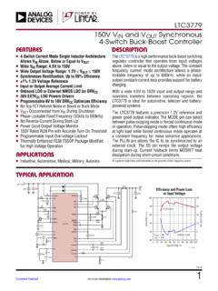
3 All other trademarks are the property of their respective (V)5 6 7 8 9 10 11 12 13 14 15 16 17 18 19 Efficiency (%)99989796959493929190 POWER LOSS (W)8076543214605 TA01b20 VOUT = 12 VILOAD = 5Af = 200kHztypical application12V/5A Buck-Boost DC/DC Module Regulator with to 20V InputEfficiency and Power Loss vs Input VoltageVOUTFCBRUNSW1SW2 RSENSESENSE F35V330 F25V4605 TA01 VOUT12V5 ACLOCK TO F10 F35V+ON/OFFSENSE+6m LTM460524605fdFor more information MaxiMuM ratingsVIN .. to 20 VVOUT .. to 16 VINTVCC, EXTVCC, RUN, SS, PGOOD .. to 7 VSW1, SW2 (Note 6) .. 5V to 20 VVFB, COMP .. to , STBYMD .. to INTVCCPLLIN .. to .. to Temper atur e Range (Note 2) .. 40 C to 85 CStorage Temper atur e Range .. 55 C to 125 C(Note 1)pin conFiguration(See Table 6.)
4 Pin Assignment)LGA PACKAGE141-LEAD (15mm 15mm )BANK 2 BANK 1 BANK 3 BANK 4 BANK 5 BANK 6 TOP VIEW1234567810911 12 LKJHGFEDCBMA TJMAX = 125 C, JP = 4 C/W WEIGHT = characteristics The l denotes the specifications which apply over the full operating temperature range, otherwise specifications are at TA = 25 C (Note 2), VIN = 12V. Per typical application (front page) SpecificationsVIN(DC)Input DC (UVLO)Undervoltage Lockout ThresholdVIN (VIN)Input Supply Bias Current Normal Standby Shutdown Supply Current VRUN = 0V, VSTBYMD > 2V VRUN = 0V, VSTBYMD = Open 35 60 mA mA AorDer inForMationPART NUMBERPAD OR BALL FINISHPART MARKING*PACKAGE TYPEMSL RATINGTEMPERATURE RANGE (SEE NOTE 2)DEVICE FINISH CODELTM4605EV#PBFAu (RoHS)LTM4605Ve4 LGA3 40 C to 85 CLTM4605IV#PBFAu (RoHS)LTM4605Ve4 LGA3 40 C to 85 CConsult Marketing for parts specified with wider operating temperature ranges.
5 *Device temperature grade is indicated by a label on the shipping container. Pad or ball finish code is per IPC/JEDEC J-STD-609. Terminal Finish Part Marking: Recommended LGA and BGA PCB Assembly and Manufacturing Procedures: LGA and BGA Package and Tray Drawings: more information characteristics The l denotes the specifications which apply over the full operating temperature range, otherwise specifications are at TA = 25 C (Note 2), VIN = 12V. Per typical application (front page) SpecificationsIOUTDCO utput Continuous Current Range (See Output Current Derating Curves for Different VIN, VOUT and TA)VIN = 12V, VOUT = 5V VIN = 6V, VOUT = 12V12 5A A VFB/VFB(NOM)Reference Voltage Line Regulation AccuracyVIN = to 20V, VCOMP = (Note 3) VFB/VFB(LOAD)Load Regulation AccuracyVCOMP = to VCOMP = to (Note 3)l %Switch SectionM1 trTurn-On Time (Note 4)
6 Drain to Source Voltage VDS = 12V, Bias Current ISW = 10mA50nsM1 tfTurn-Off TimeDrain to Source Voltage VDS = 12V, Bias Current ISW = 10mA40nsM3 trTurn-On TimeDrain to Source Voltage VDS = 12V, Bias Current ISW = 10mA25nsM3 tfTurn-Off TimeDrain to Source Voltage VDS = 12V, Bias Current ISW = 10mA20nsM2, M4 trTurn-On TimeDrain to Source Voltage VDS = 12V, Bias Current ISW = 10mA20nsM2, M4 tfTurn-Off TimeDrain to Source Voltage VDS = 12V, Bias Current ISW = 10mA20nst1dM1 Off to M2 On Delay (Note 4)Drain to Source Voltage VDS = 12V, Bias Current ISW = 10mA50nst2dM2 Off to M1 On DelayDrain to Source Voltage VDS = 12V, Bias Current ISW = 10mA50nst3dM3 Off to M4 On DelayDrain to Source Voltage VDS = 12V, Bias Current ISW = 10mA50nst4dM4 Off to M3 On DelayDrain to Source Voltage VDS = 12V, Bias Current ISW = 10mA50nsMode Transition 1M2 Off to M4 On DelayDrain to Source Voltage VDS = 12V, Bias Current ISW = 10mA220nsMode Transition 2M4 Off to M2 On DelayDrain to Source Voltage VDS = 12V, Bias Current ISW = 10mA220nsM1 RDS(ON)Static Drain-to-Source On-ResistanceBias Current ISW = M2 RDS(ON)Static Drain-to-Source On-ResistanceBias Current ISW = 3A812m M3 RDS(ON)
7 Static Drain-to-Source On-ResistanceBias Current ISW = 3A812m M4 RDS(ON)Static Drain-to-Source On-ResistanceBias Current ISW = 3A812m Oscillator and Phase-Locked LoopfNOMN ominal FrequencyVPLLFLTR = FrequencyVPLLFLTR = 0V170200220kHzfHIGHH ighest FrequencyVPLLFLTR = Input Resistance50k IPLLFLTRP hase Detector Output CurrentfPLLIN < fOSC fPLLIN > fOSC 15 15 A ALTM460544605fdFor more information characteristics The l denotes the specifications which apply over the full operating temperature range, otherwise specifications are at TA = 25 C (Note 2), VIN = 12V. Per typical application (front page) SectionVFBF eedback Reference VoltageVCOMP = Pin ON/OFF Charging CurrentVRUN = AVSTBYMD(START)Start-Up ThresholdVSTBYMD (KA)Keep-Active Power On ThresholdVSTBYMD Rising, VRUN = Continuous Continuous Pin CurrentVFCB = AVBURSTB urst Inhibit (Constant Frequency) ThresholdMeasured at FCB (BOOST, MAX)Maximum Duty Factor% Switch M4 On99%DF( buck , MAX)Maximum Duty Factor% Switch M1 On99%tON(MIN, buck )Minimum On-Time for Synchronous Switch in buck OperationSwitch M1 (Note 5)
8 200250nsRFBHIR esistor Between VOUT and VFB Internal VCC RegulatorINTVCCI nternal VCC VoltageVIN > 7V, VEXTVCC = VLDO/VLDOI nternal VCC Load RegulationICC = 0mA to 20mA, VEXTVCC = Switchover VoltageICC = 20mA, VEXTVCC VEXTVCC(HYS)EXTVCC Switchover Hysteresis300mV VEXTVCCEXTVCC Switch Drop VoltageICC = 20mA, VEXTVCC = 6V60150mVCurrent Sensing SectionVSENSE(MAX)Maximum Current Sense ThresholdBoost Mode buck Model l 95160 130190 150mV mVVSENSE(MIN, buck )Minimum Current Sense ThresholdDiscontinuous Mode 6mVISENSES ense Pins Total Source CurrentVSENSE = VSENSE+ = 0V 380 APGOOD VFBHPGOOD Upper ThresholdVFB VFBLPGOOD Lower ThresholdVFB Falling 10% VFB(HYS)PGOOD HysteresisVFB Low VoltageIPGOOD = Leakage CurrentVPGOOD = 5V1 ANote 1: Stresses beyond those listed under Absolute Maximum Ratings may cause permanent damage to the device.
9 Exposure to any Absolute Maximum Rating condition for extended periods may affect device reliability and 2: The LTM4605E is guaranteed to meet specifications from the 0 C to 85 C operating temperature range. Specifications over the 40 C to 85 C operating temperature range are assured by design, characterization and correlation with statistical process controls. The LTM4605I is guaranteed over the 40 C to 85 C operating temperature 3: The LTM4605 is tested in a feedback loop that servos VCOMP to a specified voltage and measures the resultant 4: Turn-on and turn-off time are measured using 10% and 90% levels. Transition delay time is measured using 50% 5: 100% tested at wafer level 6: Absolute Maximum Rating of 5V on SW1 and SW2 is under transient condition more information perForMance characteristics(Refer to Figure 16)LOAD CURRENT (A)0 Efficiency (%)361294605 G0618 VIN TO TO TO CURRENT (A) (%) G02 CCMDCMBURSTLOAD CURRENT (A) (%) G01 CCMDCMBURSTLOAD CURRENT (A) (%) G03 CCMDCMSKIP CYCLE958575655545352515 LOAD CURRENT (A)0 Efficiency (%)361294605 G0418 VIN TO 5 VOUT12 VIN TO 5 VOUT5 VIN TO 5 VOUT9510085759080706560 LOAD CURRENT (A)0 Efficiency (%)361294605 G0518 VIN TO TO TO vs Load Current 6 VIN to 12 VOUTE fficiency vs Load Current 12 VIN to 12 VOUTE fficiency vs Load Current 18 VIN to 12 VOUTE fficiency vs Load Current H Inductor (CCM) Efficiency vs Load Current H Inductor (CCM)
10 Efficiency vs Load Current H Inductor (CCM)Transient Response from 6 VIN to 12 VOUTT ransient Response from 12 VIN to 12 VOUTT ransient Response from 18 VIN to 12 VOUTLOAD STEP: 0A TO 3A AT CCMOUTPUT CAPS: 4x 22 F CERAMIC CAPS AND2x 180 F ELECTROLYTIC CAPS2x 15m SENSING RESISTORS200 s/DIV4605 G07 IOUT2A/DIVVOUT200mV/DIVLOAD STEP: 0A TO 3A AT CCMOUTPUT CAPS: 4x 22 F CERAMIC CAPS AND2x 180 F ELECTROLYTIC CAPS2x 15m SENSING RESISTORS200 s/DIV4605 G08 IOUT2A/DIVVOUT200mV/DIVLOAD STEP: 0A TO 4A AT CCMOUTPUT CAPS: 4x 22 F CERAMIC CAPS AND2x 180 F ELECTROLYTIC CAPS2x 15m SENSING RESISTORS200 s/DIV4605 G09 IOUT2A/DIVVOUT100mV/DIVLTM460564605fdFor more information F SOFT-START CAPOUTPUT CAPS: 4x 22 F CERAMIC CAPS AND2x 180 F ELECTROLYTIC CAPS2x 15m SENSING RESISTORS50ms/DIV4605 G10 IIN5A/DIVIL5A/DIVVOUT5 F SOFT-START CAPOUTPUT CAPS: 4x 22 F CERAMIC CAPS AND2x 180 F ELECTROLYTIC CAPS2x 15m SENSING RESISTORS50ms/DIV4605 G11 IIN2A/DIVIL5A/DIVVOUT5V/DIVtypical perForMance characteristicsStart-Up with 6 VIN to 12 VOUT at IOUT = 5 AStart-Up with 18 VIN to 12 VOUT at IOUT = 5 AShort Circuit with 6 VIN to 12 VOUT at IOUT = 5 AShort Circuit with 18 VIN to 12 VOUT at IOUT = 5 AOUTPUT CAPS: 4x 22 F CERAMIC CAPS AND2x 180 F ELECTROLYTIC CAPS2x 15m SENSING RESISTORS20 s/DIV4605 G12 IIN10A/DIVVOUT5V/DIVOUTPUT CAPS.