Transcription of LTM8078 (Rev. A)
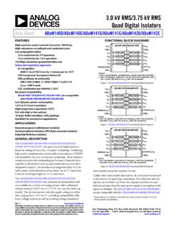
1 LTM80781 Rev. AFor more information APPLICATION FEATURESDESCRIPTIONDual , Single Step-Down Silent Switcher Module RegulatorThe LT M 8078 is 40 VIN, dual step-down Silent Switcher Module regulator. The Silent Switcher architecture minimizes EMI while delivering high efficiency at frequencies up to 3 MHz. Included in the package are the controllers, power switches, inductors, and support com-ponents. Operating over a wide input voltage range, the LTM8078 supports output voltages from to 10V, and a switching frequency range of 300kHz to 3 MHz, each set by a single resistor. Only the bulk input and output filter capacitors are needed to finish the design. The LTM8078 product video is available on LTM8078 is packaged in a compact ( ) over-molded Ball Grid Array (BGA) package suitable for automated assembly by standard surface mount equipment.
2 The LTM8078 is available with SnPb (BGA) or rohs and 5 VOUT from 7V to 40V Dual Step-Down ConverterAPPLICATIONS nTwo Complete Step-Down Switching Power Supplies nLow Noise Silent Switcher Architecture nCISPR22 Class B Compliant nCISPR25 Class 5 Compliant nWide Input Voltage Range: 3V to 40V nWide Output Voltage Range: to 10V Continuous Output Current per Channel at 24 VIN, , TA = 85 C nMultiphase Parallel Operation to Increase Current nSelectable Switching Frequency: 300kHz to 3 MHz nCompact Package ( ) Surface Mount BGA nAutomated Test Equipment nDistributed Supply Regulation nIndustrial Supplies nMedical EquipmentAll registered trademarks and trademarks are the property of their respective , VIN = 24V, BIAS = 5 VDocument Feedback1 F1 FVIN1 RUNVOUT1FB1 RTVIN2 VOUT2FB2 GNDBIAS( ) TO 40 VPINS NOT USED: TRSS1, TRSS2, PG1, PG2, CLKOUT, SYNCOMOMC8078 CURRENT (A) (%)Efficiency, VIN = 24V, BIAS = 5V8078 TA01bTA = 25 CClick to view associated Video Design AFor more information CONFIGURATIONABSOLUTE MAXIMUM RATINGSVINn, RUN, PGn.
3 42 VVOUTn, BIAS ..10 VFBn, OM, OMC, TRSSn, RT ..4 VSYNC ..6 VMaximum Internal Temperature (Note 2) ..125 CStorage Temperature .. 55 C to 125 CPeak Solder Reflow Package Body Temperature ..260 C (Note 1)VOUT2 BGA PACKAGE49-PIN ( )TJMAX = 125 C, JA = C/W, JCtop = C/W, JCbot = C/W, WEIGHT = VALUES DETERMINED PER JESD 51-9, 51-12 VIN2 RTBANK 2 BANK 1 GNDVOUT1 VIN1PG2 GNDPG1 SYNCCLKOUT7654321 ABCDEFGTRSS2 TRSS1 OMOMCRUNBIASFB1FB2 BANK 3 ORDER INFORMATIONPART NUMBERPAD OR BALL FINISHPART MARKINGPACKAGE TYPEMSL RATINGTEMPERATURE RANGE (SEE NOTE 2)DEVICE FINISH CODELTM8078EY#PBFSAC305 ( rohs )80781 BGA3 40 C to 125 CLTM8078IY#PBFLTM8078 IYSnPb (63/37)0 Device temperature grade is indicated by a label on the shipping container. Pad or ball finish code is per IPC/JEDEC J-STD-609. BGA Package and Tray Drawings This product is not recommended for second side reflow.
4 This product is moisture sensitive. For more information, go to Recommended BGA PCB Assembly and Manufacturing AFor more information CHARACTERISTICSNote 1: Stresses beyond those listed under Absolute Maximum Ratings may cause permanent damage to the device. Exposure to any Absolute Maximum Rating condition for extended periods may affect device reliability and 2: The LTM8078E is guaranteed to meet performance specifications from 0 C to 125 C internal. Specifications over the full 40 C to 125 C internal operating temperature range are assured by design, characterization and correlation with statistical process controls. The l denotes the specifications which apply over the specified operating internal temperature range, otherwise specifications are at TA = 25 C.
5 VIN1 = VIN2 = 12V, RUN = 2V unless otherwise noted (Note 2).PARAMETERCONDITIONSMINTYPMAXUNITSM inimum VIN1 Input Voltage Minimum VIN2 Input Voltage VIN1 = 3Vl VOutput DC VoltageFBn Open FBn = 10V VMaximum Output DC Current(Note 3) Current into VINnRUN = 0V BIAS = 5V, SYNC = 0V, No Load BIAS = 5V, SYNC = , No Load2 60 104 A A mACurrent into BIASRUN = 0V, BIAS = 5V BIAS = 5V, SYNC = , No Load 71 A mALine Regulation5V < VINn <40V, IOUTn = Regulation12 VINn, < IOUTn < RMS Voltage l792 784800808 816mV mVCurrent out of FBnVOUTn = 1V, FBn = 0V4 AMinimum BIAS for Proper FrequencyRT = 113k RT = RT = 300 1 3kHz MHz MHzRUN Input CurrentRUN = 0V1 APGn Threshold at FBnFBn Rising FBn Falling740 860mV mVPGn Output Sink CurrentPGn = ACLKOUT VOL0 VCLKOUT Input High Input Low Threshold to Enable Spread CurrentSYNC = 6V65 ATRSSn Source CurrentTRSSn = 0V2 ATRSSn Pull-Down ResistanceFault Condition, TRSSn = The LTM8078I is guaranteed to meet specifications over the full 40 C to 125 C internal operating temperature range.
6 Note that the maximum internal temperature is determined by specific operating conditions in conjunction with board layout, the rated package thermal resistance and other environmental factors. Note 3: The maximum current out of either channel may be limited by the internal temperature of the LTM8078 . See output current derating curves for different VIN, VOUT and AFor more information TA = 25 C, operating per Table 1,unless otherwise PERFORMANCE CHARACTERISTICSE fficiency, VOUT = BIAS = 5 VEfficiency, VOUT = BIAS = 5 VEfficiency, VOUT = BIAS = 5 VEfficiency, VOUT = BIAS = 5 VEfficiency, VOUT = BIAS = 5 VEfficiency, VOUT = BIAS = 5 VEfficiency, VOUT = BIAS = 5 VEfficiency, VOUT = BIAS = 5 VEfficiency, VOUT = BIAS = 5V, FSW = 2 MHz12 VIN24 VIN36 VINLOAD CURRENT (A) (%)BIAS = 5V8078 G0112 VIN24 VIN36 VINLOAD CURRENT (A) (%)BIAS = 5V8078 G0212 VIN24 VIN36 VINLOAD CURRENT (A) (%)BIAS = 5V8078 G0312 VIN24 VIN36 VINLOAD CURRENT (A) (%)BIAS = 5V8078 G0412 VIN24 VIN36 VINLOAD CURRENT (A) (%)
7 BIAS = 5V8078 G0512 VIN24 VIN36 VINLOAD CURRENT (A) (%)BIAS = 5V8078 G0612 VIN24 VIN36 VINLOAD CURRENT (A) (%)BIAS = 5V8078 G0712 VIN24 VIN36 VINLOAD CURRENT (A) (%)BIAS = 5V8078 G0812 VIN24 VIN36 VINLOAD CURRENT (A) (%)SW8078 G09 LTM80785 Rev. AFor more information , VOUT = 5V BIAS = 5 VEfficiency, VOUT = 5V BIAS = 5V, FSW = 2 MHzEfficiency, VOUT = 8V BIAS = 5 VEfficiency, VOUT = 10V BIAS = 5V TA = 25 C, operating per Table 1,unless otherwise PERFORMANCE CHARACTERISTICS12 VIN24 VIN36 VINLOAD CURRENT (A) (%)BIAS = 5V8078 G1012 VIN24 VIN36 VINLOAD CURRENT (A) (%)SW8078 G1112 VIN24 VIN36 VINLOAD CURRENT (A) (%)8078 G1212 VIN24 VIN36 VINLOAD CURRENT (A) (%)BIAS = 5V8078 G13 Power Loss, VOUT = BIAS = 5V, Burst Mode OperationPower Loss, VOUT = 1V BIAS = 5V, Burst Mode OperationPower Loss, VOUT = BIAS = 5V, Burst Mode OperationPower Loss, VOUT = BIAS = 5V, Burst Mode OperationPower Loss, VOUT = BIAS = 5V, Burst Mode Operation12 VIN24 VIN36 VINLOAD CURRENT (A) LOSS (W)
8 BIAS = 5V, Burst Mode8078 G1412 VIN24 VIN36 VINLOAD CURRENT (A) LOSS (W)BIAS = 5V, Burst Mode8078 G1512 VIN24 VIN36 VINLOAD CURRENT (A) LOSS (W)BIAS = 5V, Burst Mode8078 G1612 VIN24 VIN36 VINLOAD CURRENT (A) LOSS (W)BIAS = 5V, Burst Mode8078 G1712 VIN24 VIN36 VINLOAD CURRENT (A) LOSS (W)8078 G18 LTM80786 Rev. AFor more information vs Load Current VOUT = TA = 25 C, operating per Table 1,unless otherwise PERFORMANCE CHARACTERISTICSP ower Loss, VOUT = 2V BIAS = 5V, Burst Mode OperationPower Loss, VOUT = BIAS = 5V, Burst Mode OperationPower Loss, VOUT = BIAS = 5V, Burst Mode OperationPower Loss, VOUT = , 2 MHz BIAS = 5V, Burst Mode OperationPower Loss, VOUT = 5V BIAS = 5V, Burst Mode OperationPower Loss, VOUT = 5V, 2 MHz BIAS = 5V, Burst Mode OperationPower Loss, VOUT = 8V BIAS = 5V, Burst Mode OperationPower Loss, VOUT = 10V BIAS = 5V, Burst Mode Operation12 VIN24 VIN36 VINLOAD CURRENT (A) LOSS (W)BIAS = 5V, Burst Mode8078 G1912 VIN24 VIN36 VINLOAD CURRENT (A) LOSS (W)BIAS = 5V, Burst Mode8078 G2012 VIN24 VIN36 VINLOAD CURRENT (A)
9 LOSS (W)8078 G2112 VIN24 VIN36 VINLOAD CURRENT (A) LOSS (W)8078 G2212 VIN24 VIN36 VINLOAD CURRENT (A) LOSS (W)8078 G2312 VIN24 VIN36 VINLOAD CURRENT (A) LOSS (W)8078 G2412 VIN24 VIN36 VINLOAD CURRENT (A) LOSS (W)8078 G2512 VIN24 VIN36 VINLOAD CURRENT (A) LOSS (W)8078 G2612 VIN24 VIN36 VINLOAD CURRENT (A) CURRENT (A)OUT8078 G27 LTM80787 Rev. AFor more information vs Load Current VOUT = 1 VInput vs Load Current VOUT = vs Load Current VOUT = vs Load Current VOUT = vs Load Current VOUT = 2 VInput vs Load Current VOUT = vs Load Current VOUT = vs Load Current VOUT = 5 VInput vs Load Current VOUT = 8V TA = 25 C, operating per Table 1,unless otherwise PERFORMANCE CHARACTERISTICS12 VIN24 VIN36 VINLOAD CURRENT (A) CURRENT (A)VOUT = G2812 VIN24 VIN36 VINLOAD CURRENT (A) CURRENT (A)OUT8078 G2912 VIN24 VIN36 VINLOAD CURRENT (A) CURRENT (A)OUT8078 G3012 VIN24 VIN36 VINLOAD CURRENT (A) CURRENT (A)OUT8078 G3112 VIN24 VIN36 VINLOAD CURRENT (A) CURRENT (A)VOUT = G3212 VIN24 VIN36 VINLOAD CURRENT (A) CURRENT (A)8078 G3312 VIN24 VIN36 VINLOAD CURRENT (A) CURRENT (A)
10 OUT8078 G3412 VIN24 VIN36 VINLOAD CURRENT (A) CURRENT (A)OUT8078 G3512 VIN24 VIN36 VINLOAD CURRENT (A) CURRENT (A)VOUT = 8V8078 G36 LTM80788 Rev. AFor more information vs Load Current VOUT = 10 VInput Current vs VIN VOUT Short CircuitedDropout Voltage vs Load Current VOUT = 5V, BIAS = 5 VBIAS Current vs Frequency VIN = 12V, VOUT = , BIAS = 5V Forced Continuous ModeDerating, VOUT = BIAS = 5V, DC2777A Demo Board Both Channels at Same LoadtDerating, VOUT = , BIAS = 5V, DC2777A Demo Board Both Channels at Same LoadDerating, VOUT = BIAS = 5V, DC2777A Demo Board Both Channels at Same LoadDerating, VOUT = BIAS = 5V, DC2777A Demo Board Both Channels at Same LoadDerating, VOUT = , BIAS = 5V, DC2777A Demo Board Both Channels at Same Load TA = 25 C, operating per Table 1,unless otherwise PERFORMANCE CHARACTERISTICS12 VIN24 VIN36 VINLOAD CURRENT (A) CURRENT (A)VOUT = 10V8078 G37 VIN (V)