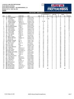
Transcription of Microprocessor Reset Circuits - Analog Devices
1 Microprocessor Reset Circuits Data Sheet ADM1810 to ADM1813/ADM1815 to ADM1818. FEATURES FUNCTIONAL BLOCK DIAGRAMS. Reliable low cost voltage monitor with Reset output ADM1810/ADM1815. VCC. Suitable for monitoring V, 3 V, V, and 5 V power supply voltages RST. Reset threshold levels: V, V, V, V, V, VCC. TOLERANCE. V, and V typical BIAS. Active high and low push-pull output choices: ADM1810, 150ms DELAY. ADM1812, ADM1815, and ADM1817 GND TC. REFERENCE. Open-drain with internal pull-up resistor output choices: ADM1811, ADM1813, ADM1816, and ADM1818. Can be used with a manual push-button to generate a Reset : ADM1811/ADM1816. ADM1813, ADM1818 VCC. Initialization of Microprocessor systems with added safety . RST. Available in 3-lead SOT-23 and SC70 packages VCC. APPLICATIONS TOLERANCE. BIAS. 150ms Microprocessor systems DELAY. Computers GND TC. REFERENCE. Controllers Intelligent instruments Automotive systems ADM1812/ADM1817. VCC. GENERAL DESCRIPTION.
2 The ADM181x range of voltage monitoring Circuits is used in RST. VCC. any application where an electronic system needs to be Reset TOLERANCE. when a voltage increases above or below a predetermined value. BIAS. 150ms DELAY. Because of the Reset delay time incorporated into the ADM181x GND TC. series, these Devices provide a safe startup for electronic systems. REFERENCE. Before a system initializes, the power supply must stabilize. Using the ADM181x series ensures that there are typically 150 ms for the power supply to stabilize before the system resets and ADM1813/ADM1818. VCC. safe system initialization begins. Reset .. RST. MONITOR. The ADM181x series of Microprocessor Reset Circuits are VCC. available in low cost, space-saving SOT-23 and SC70 packages. TOLERANCE. BIAS. 150ms DELAY. GND TC. 00064-001. REFERENCE. Figure 1. Rev. F Document Feedback Information furnished by Analog Devices is believed to be accurate and reliable. However, no responsibility is assumed by Analog Devices for its use, nor for any infringements of patents or other rights of third parties that may result from its use.
3 Specifications subject to change without notice. No One Technology Way, Box 9106, Norwood, MA 02062-9106, license is granted by implication or otherwise under any patent or patent rights of Analog Devices . Tel: 1999 2013 Analog Devices , Inc. All rights reserved. Trademarks and registered trademarks are the property of their respective owners. Technical Support ADM1810 to ADM1813/ADM1815 to ADM1818 Data Sheet TABLE OF CONTENTS. Features .. 1 Typical Performance Characteristics ..6 Applications .. 1 Theory of Operation ..7 General Description .. 1 Timing Diagrams for All Devices ..7 Functional Block Diagrams .. 1 ADM1813 and ADM1818 ..7 Revision History .. 2 ADM1810, ADM1812, ADM1815, and ADM1817 ..7 3 ADM1811 and ADM1816 ..7 Absolute Maximum 4 Outline Dimensions ..8 ESD Caution .. 4 Ordering Guide ..9 Pin Configurations and Function Descriptions .. 5 REVISION HISTORY. 10/13 Rev. E to Rev. F 2/03 Rev. A to Rev. B. Changed Open-Drain to Open-Drain with Internal Pull-Up Edits to Resistor.
4 Throughout Deleted Table I ..1. Updated Outline Dimensions .. 8 Edits to Specifications ..2. Changes to Ordering Guide .. 9 Edits to Absolute Maximum Ratings ..3. Edits to Ordering Guide ..3. 8/08 Rev. D to Rev. E Added Typical Performance Characteristics ..4. Changes to Table 3 .. 5 Edits to ADM1813 AND ADM1818 section ..5. Updated Outline Dimensions .. 8 Edits to ADM1810, ADM1812, ADM1815, and Changes to Ordering Guide .. 9 ADM1817 Section ..5. Edits to ADM1811 and ADM1816 Section ..5. 10/05 Rev. C to Rev. D Updated Outline Dimensions ..6. Updated Format .. Universal Added Figure 3 .. 5 3/02 Rev. 0 to Rev. A. Changes to Table 3 .. 5 Addition of Table ..1. Updated Outline Dimensions .. 8 Edits to Ordering Guide ..3. Edits to Ordering Guide .. 9 Addition of New Text to ADM1813 and ADM1818 Section ..4. 9/03 Rev. B to Rev. C. 4/99 Revision 0: Initial Version Added SC70 .. Universal Edits to Specifications .. 2. Edits to Ordering Guide .. 4. Updated Outline Dimensions.
5 7. Rev. F | Page 2 of 12. Data Sheet ADM1810 to ADM1813/ADM1815 to ADM1818. SPECIFICATIONS. VCC = full operating range, TA = 40 C to +105 C, unless otherwise noted. Table 1. Parameter Min Typ Max Unit Comments SUPPLY. Voltage 1 V TA = 0 C to 105 C. V TA = 40 C to +105 C. Current 9 16 A VCC = V, VCC > VTH, no load 4 10 A VCC = V, VCC > VTH, no load OUTPUT CURRENT. RST Output Source Current 350 A VCC VTH (max), Reset not asserted (ADM1810/ADM1815). RST Output Source Current 350 A VCC VTH (min), Reset asserted (ADM1812/ADM1817). RST Output Sink Current 8 mA VCC V, Reset asserted, VOUT = V (ADM1810/ADM1811/. ADM1813/ADM1815/ADM1816/ADM1818). RST Output Sink Current 8 mA VCC V, Reset not asserted, VOUT = V (ADM1812/ADM1817). OUTPUT VOLTAGE VCC VCC V ADM1810/ADM1812/ADM1815/ADM1817 at 0 A to 500 A. VCC TRIP POINT. ADM1810-5, ADM1811-5, V. ADM1812-5, ADM1813-5. ADM1810-10, ADM1811-10, V. ADM1812-10, ADM1813-10. ADM1815-5, ADM1816-5, V. ADM1817-5, ADM1818-5.
6 ADM1815-10, ADM1816-10, V. ADM1817-10, ADM1818-10. ADM1815-20, ADM1816-20, V. ADM1817-20, ADM1818-20. ADM1815-R23, ADM1816-R23, V. ADM1817-R23, ADM1818-R23. ADM1815-R22, ADM1816-R22, V. ADM1817-R22, ADM1818-R22. INTERNAL PULL-UP RESISTOR. ADM1811/ADM1816 k . ADM1813/ADM1818 k . OUTPUT CAPACITANCE 10 pF. Reset ACTIVE TIME 100 150 250 ms VCC DETECT TO Reset . Falling 10 s Rising 100 150 250 ms tR = 5 s PUSH-BUTTON DETECT TO RST 1 s ADM1813/ADM1818. PUSH-BUTTON Reset 100 150 250 ms ADM1813/ADM1818. Rev. F | Page 3 of 12. ADM1810 to ADM1813/ADM1815 to ADM1818 Data Sheet ABSOLUTE MAXIMUM RATINGS. TA = 25 C, unless otherwise noted. Stresses above those listed under Absolute Maximum Ratings Table 2. may cause permanent damage to the device. This is a stress rating only; functional operation of the device at these or any Parameter Rating other conditions above those indicated in the operational VCC V to + V. section of this specification is not implied.
7 Exposure to absolute Input Current 20 mA. maximum rating conditions for extended periods may affect Operating Temperature Range 40 C to +105 C. device reliability. Storage Temperature Range 65 C to +150 C. JA Thermal Impedance, SOT-23 270 C/W ESD CAUTION. JA Thermal Impedance, SC70 146 C/W. Lead Temperature (Soldering, 10 sec) 300 C. Vapor Phase (60 sec) 215 C. Infrared (15 sec) 220 C. Rev. F | Page 4 of 12. Data Sheet ADM1810 to ADM1813/ADM1815 to ADM1818. PIN CONFIGURATIONS AND FUNCTION DESCRIPTIONS. RST/RST 1 VCC 1. ADM181x ADM181x TOP VIEW 3 GND TOP VIEW 3 GND. (Not to Scale) (Not to Scale). 00064-002. 00064-014. VCC 2 RST/RST 2. Figure 2. 3-Lead SOT-23 Pin Configuration Figure 3. 3-Lead SC70 Pin Configuration Table 3. Pin Function Descriptions Pin No. SOT-23 SC70 Mnemonic Description 1 2 RST Active High Reset Output. RST remains high while VCC is below the Reset threshold and remains high for 150 ms typical after VCC rises above the Reset threshold.
8 Applies to the ADM1812 and ADM1817 only. RST Active Low Reset Output. RST remains low while VCC is below the Reset threshold and remains low for 150 ms typical after VCC rises above the Reset threshold. Applies to the ADM1810, ADM1811, ADM1813, ADM1815, ADM1816, and ADM1818 only. 2 1 VCC Supply Voltage. The supply voltage being monitored. 3 3 GND Ground. 0 V ground reference for all signals. Rev. F | Page 5 of 12. ADM1810 to ADM1813/ADM1815 to ADM1818 Data Sheet TYPICAL PERFORMANCE CHARACTERISTICS. 10 ICC @VCC = NORMALIZED Reset THRESHOLD. 8. 6 DEVIATION (RISE). ICC ( A). ICC @VCC = 3V. DEVIATION (FALL). 4. 2. 00064-003. 00064-006. 0 40 20 0 20 30 50 70 85 100 120 40 20 0 20 30 50 70 85 100 120. TEMPERATURE ( C) TEMPERATURE ( C). Figure 4. Supply Current vs. Temperature Figure 7. Normalized Reset Threshold vs. Temperature 900 60. 800. 50. POWER-DOWN Reset DELAY ( s). 700. MAXIMUM TRANSIENT ( s). 600 40. 500. VOD = 20mV 30. 400. 300 20. VOD = 125mV.
9 200. 10. 00064-004. 00064-007. 100. VOD = 200mV. 0 0. 40 20 0 20 30 50 70 85 100 120 10 30 40 60 80 100 200 400 600 800 1000. TEMPERATURE ( C) VTH VCC (mV). Figure 5. Power-Down Reset Delay vs. Temperature Figure 8. Maximum Transient Duration Without Causing a Reset Pulse vs. Reset Comparator Overdrive 380. 370. POWER-UP Reset TIMEOUT (ms). 360. 350. 340. 330. 320. 310. 00064-005. 300. 290. 40 20 0 20 30 50 70 85 100 120. TEMPERATURE ( C). Figure 6. Power-Up Reset Timeout vs. Temperature Rev. F | Page 6 of 12. Data Sheet ADM1810 to ADM1813/ADM1815 to ADM1818. THEORY OF OPERATION. TIMING DIAGRAMS FOR ALL Devices PUSH-BUTTON TIME. Reset TIMEOUT. The following two timing diagrams are valid for ADM1810, VOLTAGE. ADM1811, ADM1812, ADM1813, ADM1815, ADM1816, INPUT HIGH. 00064-011. ADM1817, and ADM1818. VOLTAGE. INPUT LOW. VCC. VCC TRIP POINT (MAX) Figure 12. Push-Button Reset Timing Diagram VCC TRIP POINT. VCC TRIP POINT (MIN) The ADM1818 range has V and V (typical) trip point VCC TO Reset options that allow the user to monitor V and 3 V supplies.
10 RST DELAY. For 5 V monitoring requirements, the ADM1813 range has V. and V (typical) trip point options. ADM1810, ADM1812, ADM1815, AND ADM1817. 00064-008. VOL. The ADM1812 is a 5 V supply monitor with an active high Figure 9. Power-Down Timing Diagram push-pull output and trip point options of V and V. typical. The ADM1810 is similar to the ADM1812, except that the ADM1810 has an active low push-pull output stage. The VCC TRIP POINT (MAX). ADM1817 is suitable for monitoring V, 3 V, and V. VCC TRIP POINT. VCC TRIP POINT (MIN). supplies, with an active high push-pull output and trip point VCC. options of V, V, V, V, and V typical. Reset ACTIVE TIMEOUT The ADM1815 is similar to the ADM1817, except that the ADM1815 has an active low push-pull output stage. The ADM1810/ADM1812/ADM1815/ADM1817 can connect directly to most Microprocessor Reset inputs without the need 00064-009. RST. for external components. VCC. Figure 10. Power-Up Timing Diagram ADM1813 AND ADM1818 ADM1810/.