Transcription of Multiple Output, High Precision, Dual-Tracking Reference ...
1 Multiple Output, High precision , Dual-Tracking Reference Data Sheet AD588 Rev. M Document Feedback Information furnished by Analog Devices is believed to be accurate and reliable. However, no responsibility is assumed by Analog Devices for its use, nor for any infringements of patents or other rights of third parties that may result from its use. Specifications subject to change without notice. No license is granted by implication or otherwise under any patent or patent rights of Analog Devices. Trademarks and registered trademarks are the property of their respective owners. One Technology Way, Box 9106, Norwood, MA 02062-9106, Tel: 1986 2015 Analog Devices, Inc. All rights reserved. Technical Support FEATURES Low drift: ppm/ C Low initial error: 1 mV pin programmable output +10 V, +5 V, 5 V tracking, 5 V, 10 V Flexible output force and sense terminals High impedance ground sense 16-lead SOIC package and 16-lead CERDIP MIL-STD-883-compliant versions available GENERAL DESCRIPTION The AD588 represents a major advance in state-of-the-art monolithic voltage references.
2 Low initial error and low temperature drift give the AD588 absolute accuracy performance previously not available in monolithic form. The AD588 uses a proprietary ion-implanted, buried Zener diode and laser-wafer drift trimming of high stability thin film resistors to provide outstanding performance. The AD588 includes the basic Reference cell and three additional amplifiers that provide pin programmable output ranges. The amplifiers are laser trimmed for low offset and low drift to maintain the accuracy of the Reference . The amplifiers are configured to allow Kelvin connections to the load and/or boosters for driving long lines or high current loads, delivering the full accuracy of the AD588 where it is required in the application circuit. The low initial error allows the AD588 to be used as a system Reference in precision measurement applications requiring 12-bit absolute accuracy.
3 In such systems, the AD588 can provide a known voltage for system calibration in software. The low drift also allows compensation for the drift of other components in a system. Manual system calibration and the cost of periodic recalibration can, therefore, be eliminated. Furthermore, the mechanical instability of a trimming potentiometer and the potential for improper calibration can be eliminated by using the AD588 in conjunction with auto calibration software. The AD588 is available in seven versions. The AD588JQ and AD588KQ are packaged in a 16-lead CERDIP and are specified for 0 C to +70 C operation. The AD588AQ and AD588BQ are packaged in a 16-lead CERDIP, and the AD588 ARWZ is packaged in a 16-lead SOIC, and they are specified for the 25 C to +85 C industrial temperature range. The ceramic AD588TE and AD588TQ grades are specified for the full military/aerospace temperature range.
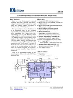
4 FUNCTIONAL BLOCK DIAGRAM R3 RBR1R2R4R5R6 GAINADJGNDSENSE+INGNDSENSE INVLOWBALADJVCTA4 IN VS+VSA4 OUTFORCEA4 OUTSENSEA3 OUTFORCEA3 OUTSENSEA3 INVHIGHNOISEREDUCTIONA1A4AD58800531-001A 313111281095114152163467A2 Figure 1. PRODUCT HIGHLIGHTS 1. The AD588 offers 12-bit absolute accuracy without any user adjustments. Optional fine-trim connections are provided for applications requiring higher precision . The fine trimming does not alter the operating conditions of the Zener or the buffer amplifiers, and so does not increase the temperature drift. 2. Output noise of the AD588 is very low, typically 6 V p-p. A pin is provided for additional noise filtering using an external capacitor. 3. A precision 5 V tracking mode with Kelvin output connections is available with no external components. Tracking error is less than 1 mV, and a fine trim is available for applications requiring exact symmetry between the +5 V and 5 V outputs.
5 4. Pin strapping capability allows configuration of a wide variety of outputs: 5 V, +5 V, +10 V, 5 V, and 10 V dual outputs or +5 V, 5 V, +10 V, and 10 V single outputs. AD588 Data Sheet Rev. M | Page 2 of 20 TABLE OF CONTENTS Features .. 1 General Description .. 1 Functional Block Diagram .. 1 Product Highlights .. 1 Revision History .. 2 Specifications .. 3 Absolute Maximum Ratings .. 4 ESD Caution .. 4 Pin Configuration and Function Descriptions .. 5 Theory of Operation .. 6 Applications Information .. 7 Calibration .. 7 Noise Performance and Reduction .. 9 Tu r n-On Time .. 10 Temperature 10 Kelvin Connections .. 11 Dynamic Performance .. 13 Using the AD588 with Converters .. 15 AD7535 14-Bit Digital-to -Analog Converter .. 15 AD569 16-Bit Digital-to -Analog Converter .. 15 Substituting for Internal References .. 16 AD574A 12-Bit Analog-to -Digital Converter .. 16 Resistance Temperature Detector (RTD) Excitation.
6 16 Boosted precision Current Source .. 17 Bridge Driver Circuits .. 17 Outline Dimensions .. 19 Ordering Guide .. 19 REVISION HISTORY 11/15 Rev. L to Rev. M Changes to Figure 13 .. 11 10/10 Rev. K to Rev. L Changes to Amplifier A2 Plus and Minus Input Labels in Figures .. Throughout 9/10 R e v. J t o R e v. K Changes to Product Title .. 1 4/10 R e v. I t o R e v. J Changes to Calibration Section .. 8 11/09 R e v. H t o R e v. I Changes to Figure 40 and Figure 41 .. 18 10/09 R e v. G t o R e v. H Changes to General Description Section .. 1 6/06 R e v. F t o R e v. G Changes to Table 5 .. 7 Updated Outline Dimensions .. 19 3/06 R e v. E t o R e v. F Replaced Figure 5 .. 8 Updated Outline Dimensions .. 19 11/05 R e v. D t o R e v. E Updated Format .. Universal Added SOIC Version .. Universal Changes to Pin 14 in Figures.
7 Universal Changes to Pin 9 and Pin 10 in Figures .. Universal Changes to Specifications Section .. 3 Added Table 3 .. 4 Added Pin Configuration and Function Descriptions Section .. 5 Added Table 4 .. 5 Changes to Grade in Reference and in Figure 12 .. 11 Updated Outline Dimensions .. 19 Changes to Ordering Guide .. 19 2/03 R e v. C t o R e v. D Added KQ Model and Deleted SQ and TQ Models .. Universal Changes to General Description .. 1 Change to Product Highlights .. 1 Changes to Specifications .. 2 Changes to Ordering Guide .. 3 Updated Outline Dimensions .. 15 10/02 Rev. B to Rev. C Changes to General Description .. 1 Changes to Specifications .. 2 Changes to Ordering Guide .. 3 Changes to Table 1 .. 5 Deleted Figure 10c .. 7 Updated Outline Dimensions .. 15 Data Sheet AD588 Rev. M | Page 3 of 20 SPECIFICATIONS Typical at 25 C, 10 V output, VS = 15 V, unless otherwise noted.
8 Specifications shown in boldface are tested on all production units at final electrical test. Results from those tests are used to calculate outgoing quality levels. All minimum and maximum specifications are guaranteed, although only those shown in boldface are tested on all production units. Table 1. AD588JQ/AD588AQ AD588BQ/AD588KQ AD588 ARWZ Parameter1 Min Typ Max Min Typ Max Min Typ Max Unit OUTPUT voltage ERROR +10 V, 10 V Outputs 3 1 +1 5 +5 mV +5 V, 5 V Outputs 3 1 +1 5 +5 mV 5 V TRACKING MODE Symmetry Error mV OUTPUT voltage DRIFT 0 C to 70 C (J, K, B) 2 3 2 3 ppm/ C 25 C to +85 C (A, B) 3 3 3 ppm/ C GAIN ADJ AND BAL ADJ2 Trim Range 4 4 4 mV Input Resistance 150 150 150 k LINE REGULATION TMIN to TMAX3 200 200 200 V/V LOAD REGULATION TMIN to TMAX +10 V Output, 0 mA < IOUT < 10 mA 50 50 50 V/mA 10 V Output, 10 mA < IOUT < 0 mA 50 50 50 V/mA SUPPLY CURRENT TMIN to TMAX 6 10 6 10 6 10 mA Power Dissipation 180 300 180 300 180 300 mW OUTPUT NOISE (Any Output) Hz to 10 Hz 6 6 6 V p-p Spectral Density, 100 Hz 100 100 100 nV/ Hz LONG-TERM STABILITY (at 25 C)
9 15 15 15 ppm/1000 hr BUFFER AMPLIFIERS Offset voltage 100 10 100 V Offset voltage Drift 1 1 1 V/ C Bias Current 20 20 20 nA Open-Loop Gain 110 110 110 dB Output Current (A3, A4) 10 +10 10 +10 10 +10 mA Common-Mode Rejection (A3, A4) VCM = 1 V p-p 100 100 100 dB Short Circuit Current 50 50 50 mA TEMPERATURE RANGE Specified Performance J, K Grades 0 70 0 70 C A, B Grades 25 +85 25 +85 25 +85 C 1 Specifications tested using 5 V configuration, unless otherwise indicated. See Figure 4 through Figure 6 for output configurations at +10 V, 10 V, +5 V, 5 V and 5 V. 2 Gain and balance adjustments guaranteed capable of trimming output voltage error and symmetry error to zero. 3 For 10 V output, VS can be as low as 12 V. See Table 3 for test conditions at various voltages.
10 AD588 Data Sheet Rev. M | Page 4 of 20 ABSOLUTE MAXIMUM RATINGS Table 2. Parameter Rating +VS to VS 36 V Power Dissipation (25 C) 600 mW Storage Temperature Range 65 C to +150 C Lead Temperature (Soldering 10 sec) 300 C Package Thermal Resistance ( JA/ JC) 90 C/25 C/W Output Protection All outputs safe if shorted to ground Table 3. Test Conditions voltage Conditions +10 V Output VS = 15 V, + V +VS +18 V 10 V Output 18 V VS V, +VS = +15 V 5 V Output +VS = +18 V, VS = 18 V +VS = + V, VS = V Stresses at or above those listed under Absolute Maximum Ratings may cause permanent damage to the product. This is a stress rating only; functional operation of the product at these or any other conditions above those indicated in the operational section of this specification is not implied. Operation beyond the maximum operating conditions for extended periods may affect product reliability.