Transcription of OneTechnologyWay P.O.Box9106 Norwood,MA …
1 AN-1026 APPLICATION NOTE One Technology Way P. O . Box 9106 Norwood, MA 02062-9106, Tel: Fax: High Speed Differential ADC Driver Design Considerations by John Ardizzoni and Jonathan Pearson Rev. A | Page 1 of 13 INTRODUCTION Most modern high performance analog-to-digital converters (ADCs) use differential inputs to reject common -mode noise and interference, increase dynamic range by a factor of 2, and improve overall performance due to balanced signaling. Though ADCs with differential inputs can accept single-ended input signals, optimum ADC performance is achieved when the input signal is differential. ADC drivers circuits often specifically designed to provide such signals perform many important functions, including amplitude scaling, single-ended to differential conversion, buffering, common -mode offset adjustment, and filtering. Since the introduction of the AD8138, differential ADC drivers have become essential signal conditioning elements in data acquisition systems.
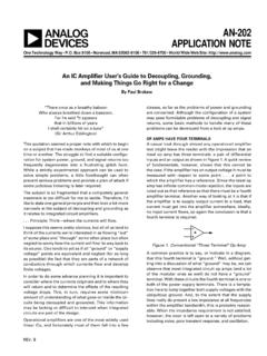
2 VAVARF1RF2 VIPVIN, dmVIN+ VOCMRG1RG2 VOUT, dmVONVOP +08263-001 Figure 1. Differential Amplifier A basic fully differential voltage feedback ADC driver is shown in Figure 1. Two d ifferences from a traditional op amp feedback circuit can be seen. The differential ADC driver has an additional output terminal (VON) and an additional input terminal (VOCM). These terminals provide great flexibility when interfacing signals to ADCs that have differential inputs. Instead of a single-ended output, the differential ADC driver produces a balanced differential output, with respect to VOCM, between VOP and VON (P indicates positive and N indicates negative). The VOCM input controls the output common -mode voltage. As long as the inputs and outputs stay within their specified limits, the output common -mode voltage must equal the voltage applied to the VOCM input. Negative feedback and high open-loop gain cause the voltages at the amplifier input terminals, VA+ and VA , to be essentially equal.
3 For the discussions that follow, some definitions are in order. If the input signal is balanced, VIP and VIN are nominally equal in amplitude and opposite in phase with respect to a common reference voltage. When the input is single-ended, one input is at a fixed voltage, and the other varies with respect to it. In either case, the input signal is defined as VIP VIN. The differential-mode input voltage (VIN, dm) and the common -mode input voltage (VIN, cm) are defined in Equation 1 and Equation 2. VIN, dm = VIP VIN (1) VIN, cm = 2 INIPVV+ (2) This common -mode definition is intuitive when applied to balanced inputs, but it is also valid for single-ended inputs. The output also has a differential mode and a common mode, defined in Equation 3 and Equation 4. VOUT, dm = VOP VON (3) VOUT, cm = 2 ONOPVV+ (4) Note the difference between the actual output common -mode voltage (VO U T, c m) and the VOCM input terminal, which establishes the output common -mode level.
4 The analysis of the differential ADC drivers is considerably more complex than that of traditional op amps. To simplify the algebra, it is expedient to define two feedback factors, 1 and 2, as given in Equation 5 and Equation 6. G1F1G11 RRR += (5) 2222 GFGRRR += (6) AN-1026 Application Note Rev. A | Page 2 of 13 TABLE OF CONTENTS Introduction .. 1 Revision History .. 2 Terminating the Input to an ADC Driver .. 3 Input common -Mode Voltage Range (ICMVR) .. 5 Input and Output Coupling: AC or 6 Output Swing .. 7 Noise .. 7 Supply Voltage ..9 Harmonic Distortion .. 10 Bandwidth and Slew Rate .. 11 Stability .. 11 PCB Layout .. 12 REVISION HISTORY 11/15 Rev. 0 to Rev. A Changes to Terminating the Input to an ADC Driver Section and Input common -Mo d e Vo l t age Range (ICMVR) Section .. 5 Changes to Noise Section .. 9 Added Figure 22; Renumbered Sequentially .. 13 Changes to Figure 23 .. 13 11/09 Revision 0: Initial Version Application Note AN-1026 Rev.
5 A | Page 3 of 13 In most ADC driving applications, 1 = 2, but the general closed-loop equation for VO U T, d m, in terms of VIP, VIN, VOCM, 1, and 2, is useful to gain insight into how beta mismatch affects performance. The equation for VO U T, d m, shown in Equation 7, includes the finite frequency dependent, open-loop voltage gain of the amplifier, A(s). ()()()( )() ++ + +=212IN1IP21 OCM21 OUT,dm sA V V V V21112(7) When 1 2, the differential output voltage depends on VOCM, which is an undesirable outcome because it produces an offset and excess noise in the differential output. The gain bandwidth product of the voltage-feedback architecture is constant. The gain in the gain bandwidth product is the reciprocal of the averages of the two feedback factors. When 1 = 2 , Equation 7 reduces to Equation 8. ( ) + =)(111,,sARRVVGFdmINdmOUT (8) Equation 8 is a more familiar looking expression; the ideal closed-loop gain becomes simply RF/RG when A(s) approaches.
6 The gain bandwidth product is also more familiar looking, with the noise gain equal to 1/ , just as with a traditional op amp. The ideal closed-loop gain for a differential ADC driver with matched feedback factors is seen in Equation 9. GFdmINdmOUTVRRVVA==,, (9) Output balance, an important performance metric for differential ADC drivers, has two components: amplitude balance and phase balance. Amplitude balance is a measure of how closely the two outputs are matched in amplitude; in an ideal amplifier, they are exactly matched. Output phase balance is a measure of how close the phase difference between the two outputs is to 180 . Any imbalance in output amplitude or phase produces an undesirable common -mode component in the output. The output balance error (see Equation 10) is the log ratio of the output common -mode voltage produced by a differential input signal to the output differential-mode voltage produced by the same input signal, expressed in decibels.
7 =dmOUTcmOUTVVE rrorBalanceOutput,,10log20 (10) An internal common -mode feedback loop forces VO U T, c m to equal the voltage applied to the VOCM input, producing excellent output balance. TERMINATING THE INPUT TO AN ADC DRIVER ADC drivers are frequently used in systems that process high speed signals. Devices separated by more than a small fraction of a signal wavelength must be connected by electrical transmission lines with controlled impedance to avoid losing signal integrity. Optimum performance is achieved when a transmission line is terminated at both ends in its characteristic impedance. The driver is generally placed close to the ADC; therefore, controlled impedance connections are not required between them. However, the incoming signal connection to the ADC driver input is often long enough to require a controlled impedance connection, terminated in the proper resistance. The input resistance of the ADC driver, whether differential or single-ended, must be greater than or equal to the desired termination resistance so that a termination resistor, RT, can be added in parallel with the amplifier input to achieve the required resistance.
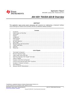
8 All ADC drivers in the examples considered here are designed to have balanced feedback ratios, as shown in Figure 2. RFRFRIN, dmVOCMRGRG08263-002 Figure 2. Differential Amplifier Input Impedance Because the voltage between the two amplifier inputs is driven to a null by negative feedback, they are virtually connected, and the differential input resistance, RIN, is simply 2 RG. To m a t c h the transmission line resistance (RL), place the RT resistor, as calculated in Equation 11, across the differential input. Figure 3 shows typical resistances RF = RG = 200 , desired RL, dm = 100 , and RT = 133 . INLTRRR111 = (11) 200 200 RL, dm = 100 VOCM200 200 RT= 133 =400 1100 11RT08263-003 Figure 3. Matching a 100 Line AN-1026 Application Note Rev. A | Page 4 of 13 Terminating a single-ended input requires significantly more effort. Figure 4 illustrates how an ADC driver operates with a single-ended input and a differential output.
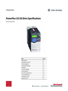
9 2V0V RF500 VOCMVOUT, RG500 VINVONVOP +08263-004 Figure 4. Example of Single-Ended Input to ADC Driver Although the input is single-ended, VIN, dm is equal to VIN. Because the RF and RG resistors are equal and balanced, the gain is unity, and the differential output, VOP VON, is equal to the input, that is, 4 V p-p. VO U T, c m is equal to VOCM = V and, from the lower feedback circuit, input voltages VA+ and VA are equal to VOP/2. Using Equation 3 and Equation 4, VOP = VOCM + VIN/2, an in-phase swing of 1 V about V. VON = VOCM VIN/2, an antiphase swing of 1 V about V. Thus, VA+ and VA swing V about V. The ac component of the current that must be supplied by VIN is (2 V V)/500 = 3 mA; therefore, the resistance to ground that must be matched, looking in from VIN, is 667 . The general formula for determining this single-ended input resistance, when the feedback factors of each loop are matched, is shown in Equation 12, where RIN, se is the single-ended input resistance.
10 () + =FGFGseINRRRRR21, (12) This equation is a starting point for calculating the termination resistance. However, it is important to note that amplifier gain equations are based on the assumption of a zero impedance input source. A significant source impedance that must be matched in the presence of an imbalance caused by a single-ended input inherently adds resistance only to the upper RG. To retain the balance, this must be matched by adding resistance to the lower RG, but this affects the gain. Although it may be possible to determine a closed form solution to the problem of terminating a single-ended signal, an iterative method is generally used. The need for it is apparent in the following example. In Figure 5, a single-ended to differential gain of 1, a 50 input termination, and feedback and gain resistors with values in the neighborhood of 200 are required to keep noise low. 200 200 VOCMVOUT, 200 267 VONVOP +08263-005 Figure 5.