Transcription of PCA9546A 4-channel I2C-bus switch with reset
1 PCA9546A . 4-channel I2C-bus switch with reset Rev. 6 30 April 2014 Product data sheet 1. General description The PCA9546A is a quad bidirectional translating switch controlled via the I2C-bus . The SCL/SDA upstream pair fans out to four downstream pairs, or channels. Any individual SCx/SDx channel or combination of channels can be selected, determined by the contents of the programmable control register. An active LOW reset input allows the PCA9546A to recover from a situation where one of the downstream I2C-buses is stuck in a LOW state.
2 Pulling the reset pin LOW resets the I2C-bus state machine and causes all the channels to be deselected as does the internal Power-On reset (POR) function. The pass gates of the switches are constructed such that the VDD pin can be used to limit the maximum high voltage which is passed by the PCA9546A . This allows the use of different bus voltages on each pair, so that V or V or V parts can communicate with 5 V parts without any additional protection. External pull-up resistors pull the bus up to the desired voltage level for each channel.
3 All I/O pins are 5 V tolerant. 2. Features and benefits 1-of-4 bidirectional translating switches I2C-bus interface logic; compatible with SMBus standards Active LOW reset input 3 address pins allowing up to 8 devices on the I2C-bus Channel selection via I2C-bus , in any combination Power-up with all switch channels deselected Low Ron switches Allows voltage level translation between V, V, V and 5 V buses No glitch on power-up Supports hot insertion Low standby current Operating power supply voltage range of V to V. 5 V tolerant Inputs 0 Hz to 400 kHz clock frequency ESD protection exceeds 2000 V HBM per JESD22-A114 and 1000 V CDM per JESD22-C101.
4 Latch-up testing is done to JEDEC Standard JESD78 which exceeds 100 mA. Three packages offered: SO16, TSSOP16, and HVQFN16. NXP Semiconductors PCA9546A . 4-channel I2C-bus switch with reset 3. Ordering information Table 1. Ordering information Type number Topside Package marking Name Description Version PCA9546 ABS 546A HVQFN16 plastic thermal enhanced very thin quad flat package; SOT629-1. no leads; 16 terminals; body 4 4 mm PCA9546AD PCA9546AD SO16 plastic small outline package; 16 leads; body width mm SOT109-1. PCA9546 APW PA9546A TSSOP16 plastic thin shrink small outline package; 16 leads; SOT403-1.
5 Body width mm Ordering options Table 2. Ordering options Type number Orderable part Package Packing method Minimum Temperature range number order quantity PCA9546 ABS PCA9546 ABS,118 HVQFN16 Reel 13 Q1/T1 6000 Tamb = 40 C to +85 C. *Standard mark SMD. PCA9546AD PCA9546AD,112 SO16 Standard marking 1000 Tamb = 40 C to +85 C. * IC's tube - DSC bulk pack PCA9546AD,118 SO16 Reel 13 Q1/T1 2500 Tamb = 40 C to +85 C. *Standard mark SMD. PCA9546 APW PCA9546 APW,112 TSSOP16 Standard marking 2400 Tamb = 40 C to +85 C. * IC's tube - DSC bulk pack PCA9546 APW,118 TSSOP16 Reel 13 Q1/T1 2500 Tamb = 40 C to +85 C.
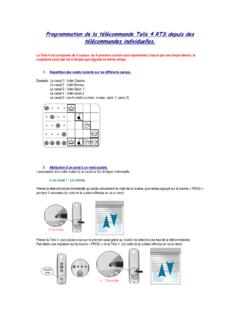
6 *Standard mark SMD. PCA9546A All information provided in this document is subject to legal disclaimers. NXP Semiconductors 2014. All rights reserved. Product data sheet Rev. 6 30 April 2014 2 of 30. NXP Semiconductors PCA9546A . 4-channel I2C-bus switch with reset 4. Block diagram PCA9546A . SC0. SC1. SC2. SC3. SD0. SD1. SD2. SD3. VSS switch CONTROL LOGIC. VDD POWER-ON. reset reset . SCL A0. INPUT. FILTER I2C-bus . SDA A1. CONTROL. A2. 002aab188. Fig 1. Block diagram of PCA9546A . PCA9546A All information provided in this document is subject to legal disclaimers.
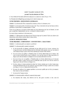
7 NXP Semiconductors 2014. All rights reserved. Product data sheet Rev. 6 30 April 2014 3 of 30. NXP Semiconductors PCA9546A . 4-channel I2C-bus switch with reset 5. Pinning information Pinning A0 1 16 VDD. A1 2 15 SDA. reset 3 14 SCL. A0 1 16 VDD. SD0 4 13 A2 A1 2 15 SDA. PCA9546AD reset 3 14 SCL. SC0 5 12 SC3. SD0 4 13 A2. PCA9546 APW. SD1 6 11 SD3 SC0 5 12 SC3. SD1 6 11 SD3. SC1 7 10 SC2. SC1 7 10 SC2. VSS 8 9 SD2 VSS 8 9 SD2. 002aab185 002aab186. Fig 2. Pin configuration for SO16 Fig 3. Pin configuration for TSSOP16. 13 SDA. 14 VDD.
8 Terminal 1. 16 A1. 15 A0. index area reset 1 12 SCL. SD0 2 11 A2. PCA9546 ABS. SC0 3 10 SC3. SD1 4 9 SD3. 7. 5. 6. 8. SC1. VSS. SD2. SC2. 002aab187. Transparent top view Fig 4. Pin configuration for HVQFN16 (transparent top view). PCA9546A All information provided in this document is subject to legal disclaimers. NXP Semiconductors 2014. All rights reserved. Product data sheet Rev. 6 30 April 2014 4 of 30. NXP Semiconductors PCA9546A . 4-channel I2C-bus switch with reset Pin description Table 3. Pin description Symbol Pin Description SO16, TSSOP16 HVQFN16.
9 A0 1 15 address input 0. A1 2 16 address input 1. reset 3 1 active LOW reset input SD0 4 2 serial data 0. SC0 5 3 serial clock 0. SD1 6 4 serial data 1. SC1 7 5 serial clock 1. VSS 8 6[1] supply ground SD2 9 7 serial data 2. SC2 10 8 serial clock 2. SD3 11 9 serial data 3. SC3 12 10 serial clock 3. A2 13 11 address input 2. SCL 14 12 serial clock line SDA 15 13 serial data line VDD 16 14 supply voltage [1] HVQFN16 package die supply ground is connected to both the VSS pin and the exposed center pad. The VSS pin must be connected to supply ground for proper device operation.
10 For enhanced thermal, electrical, and board-level performance, the exposed pad must be soldered to the board using a corresponding thermal pad on the board, and for proper heat conduction through the board thermal vias must be incorporated in the PCB in the thermal pad region. 6. Functional description Refer to Figure 1 Block diagram of PCA9546A . Device address Following a START condition, the bus master must output the address of the slave it is accessing. The address of the PCA9546A is shown in Figure 5. To conserve power, no internal pull-up resistors are incorporated on the hardware selectable address pins and they must be pulled HIGH or LOW.