Transcription of Positive Regulators Adjustable - analog.com
1 LT1117 APPLICATION FEATURESDESCRIPTION800mA Low DropoutPositive Regulators Adjustable and Fixed , , 5 VThe LT 1117 is a Positive low dropout regulator designed to provide up to 800mA of output current. The device is available in an Adjustable version and fixed output voltages of , and 5V. The version is designed specifically to be used in Active Terminators for the SCSI bus. All internal circuitry is designed to operate down to 1V input to output differential. Dropout voltage is guaranteed at a maximum of at 800mA, decreasing at lower load currents. On chip trimming adjusts the reference/output voltage to within 1%. Current limit is also trimmed in order to minimize the stress on both the regulator and the power source circuitry under overload low profi le surface mount SOT-223 package allows the device to be used in applications where space is limited. The LT1117 requires a minimum of 10 F of output capacitance for stability.
2 Output capacitors of this size or larger are normally included in most regulator designs. Unlike PNP type Regulators where up to 10% of the output current is wasted as quiescent current, the quiescent current of the LT1117 fl ows into the load, increasing effi Voltage (VIN VOUT) APPLICATIONSn Space Saving SOT-223 Surface Mount Packagen 3-Terminal Adjustable or Fixed , , 5Vn Output Current of 800mAn Operates Down to 1V Dropoutn Guaranteed Dropout Voltage at Multiple Current Levelsn Line Regulation Maxn Load Regulation Maxn Active SCSI Terminatorsn High Effi ciency Linear Regulatorsn Post Regulators for Switching Suppliesn Battery Chargersn 5V to Linear RegulatorsL, LT, LTC, LTM, Linear Technology, OPTI-LOOP and the Linear logo are registered trademarks of Linear Technology Corporation. UltraFast is a trademark of Linear Technology Corporation. All other trademarks are the property of their respective owners.
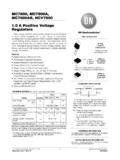
3 OUTPUT CURRENT (mA)00 DROPOUT VOLTAGE (V) 300500700TJ = 25 CTJ = 125 C INDICATES GUARANTEED TEST POINT0 C TJ 125 C 40 C TJ < 0 C18 TO 27 LINES1117 TA0110 F110 110 110 110 ++Active Terminator for SCSI-2 BusLT1117 MAXIMUM RATINGSI nput Voltage Operating Voltage LT1117, , LT1117-5 ..15V ..10V Surge Voltage LT1117, , LT1117-5 ..20V(Note 1)FRONT VIEWTAB ISVOUTINOUTADJ/GNDST PACKAGE3-LEAD PLASTIC SOT-223321 TJMAX = 125 C, JC = 15 C/WM PACKAGE3-LEAD PLASTIC DD-PAKFRONT VIEW321 INOUTADJ/GNDTAB ISVOUTTJMAX = 125 C, JC = 10 C/WPIN CONFIGURATIONORDER INFORMATIONLEAD FREE FINISHTAPE AND REELPART MARKINGPACKAGE DESCRIPTIONTEMPERATURE RANGELT1117 CST#PBFLT1117 CST#TRPBF11173-Lead Plastic SOT-2230 C to 125 CLT1117 IST#PBFLT1117 IST#TRPBF1117I3-Lead Plastic SOT-223 40 C to 125 # #TRPBF111723-Lead Plastic SOT-2230 C to 125 # #TRPBF1117I23-Lead Plastic SOT-223 40 C to 125 # #TRPBF111733-Lead Plastic SOT-2230 C to 125 # #TRPBF1117I33-Lead Plastic SOT-223 40 C to 125 CLT1117 CST-5#PBFLT1117 CST-5#TRPBF111753-Lead Plastic SOT-2230 C to 125 CLT1117 IST-5#PBFLT1117 IST-5#TRPBF1117I53-Lead Plastic SOT-223 40 C to 125 CLT1117CM#PBFLT1117CM#TRPBFLT1117CM3-Lea d Plastic DD-PAK0 C to 125 # # Plastic DD-PAK0 C to 125 # # Plastic DD-PAK0 C to 125 CLT1117CM-5#PBFLT1117CM-5#TRPBFLT1117CM- 53-Lead Plastic DD-PAK0 C to 125 COperating JunctionTemperature Range C Grade.
4 0 C to 125 C I Grade .. 40 C to 125 CStorage Temperature Range .. 65 C to 150 CLead Temperature ..(See Soldering Methods)LT1117 CHARACTERISTICSPARAMETERCONDITIONSMINTYP MAXUNITSR eference VoltageLT1117 IOUT = 10mA, (VIN VOUT) = 2V, TJ = 25 C10mA IOUT 800mA, (VIN VOUT) = 10mA, VIN = , TJ = 25 C0 IOUT 800mA, VIN 10V0 IOUT 500mA, VIN = = 10mA, VIN = 5V, TJ = 25 C0 IOUT 800mA, VIN = 10mA, VIN = 7V, TJ = 25 C0 IOUT 800mA, VIN = 10mA, VIN VOUT 15V (Note 2)IOUT = 0mA, VIN 10V (Note 2)IOUT = 0mA, VIN 15V (Note 2)IOUT = 0mA, VIN 15V (Note 2) (VIN VOUT) = 3V, 10mA IOUT 800mA (Note 2)VIN = , 0 IOUT 800mA (Note 2)VIN = , 0 IOUT 800mA (Note 2)VIN = , 0 IOUT 800mA (Note 2) VoltageIOUT = 100mA, 0 C TJ 125 C (Note 3)IOUT = 500mA, 0 C TJ 125 C (Note 3)IOUT = 800mA, 0 C TJ 125 C (Note 3) = 100mA, 40 C TJ < 0 C (Note 3)IOUT = 500mA, 40 C TJ < 0 C (Note 3)IOUT = 800mA, 40 C TJ < 0 C (Note 3) Limit(VIN VOUT)
5 = 5V, TJ = 25 C8009501200mAMinimum Load CurrentLT1117(VIN VOUT) = 15V (Note 4) The l denotes the specifications which apply over the full operating temperature range, otherwise specifications are at TJ = 25 BASED FINISHTAPE AND REELPART MARKINGPACKAGE DESCRIPTIONTEMPERATURE RANGELT1117 CSTLT1117 CST#TR11173-Lead Plastic SOT-2230 C to 125 CLT1117 ISTLT1117 IST#TR1117I3-Lead Plastic SOT-223 40 C to 125 #TR111723-Lead Plastic SOT-2230 C to 125 #TR1117I23-Lead Plastic SOT-223 40 C to 125 #TR111733-Lead Plastic SOT-2230 C to 125 #TR1117I33-Lead Plastic SOT-223 40 C to 125 CLT1117 CST-5LT1117 CST-5#TR111753-Lead Plastic SOT-2230 C to 125 CLT1117 IST-5LT1117 IST-5#TR1117I53-Lead Plastic SOT-223 40 C to 125 CLT1117 CMLT1117CM#TRLT1117CM3-Lead Plastic DD-PAK0 C to 125 # Plastic DD-PAK0 C to 125 # Plastic DD-PAK0 C to 125 CLT1117CM-5LT1117CM-5#TRLT1117CM-53-Lead Plastic DD-PAK0 C to 125 CConsult LTC Marketing for parts specified with wider operating temperature more information on lead free part marking, go to: For more information on tape and reel specifications, go to.
6 INFORMATIONLT1117 Operating Current( Adjustable Device)Short-Circuit CurrentLoad RegulationINPUT/OUTPUT DIFFERENTIAL (V)00 MINIMUM OPERATING CURRENT (mA)1341015201117 G015TJ = 25 CTJ = 125 CTJ = 55 C2 INPUT/OUTPUT DIFFERENTIAL (V)00 SHORT CIRCUIT CURRENT (A) = 25 CTJ = 125 CTEMPERATURE ( C) 50 VOLTAGE DEVIATION (%) 2525100 ILOAD = 800mAPARAMETERCONDITIONSMINTYPMAXUNITSQ uiescent 10 VVIN 15 VVIN 15 Vlll555101010mAmAmAThermal RegulationTA = 25 C, 30ms RejectionfRIPPLE = 120Hz, (VIN VOUT) = 3V, VRIPPLE = 1VP-Pl6075dBAdjust Pin Currentl55120 AAdjust Pin Current Change10mA IOUT 800mA, (VIN VOUT) ATemperature Term StabilityTA = 125 C, Output Noise(% of VOUT), 10Hz f Resistance(Junction-to-Case, at Tab)15 C/WNote 1: Stresses beyond those listed under Absolute Maximum Ratings may cause permanent damage to the device. Exposure to any Absolute Maximum Rating condition for extended periods may affect device reliability and 2: See thermal regulation specification for changes in output voltage due to heating effects.
7 Load regulation and line regulation are measured at a constant junction temperature by low duty cycle pulse 3: Dropout voltage is specified over the full output current range of the device. Dropout voltage is defined as the minimum input/output differential measured at the specified output current. Test points and limits are also shown on the Dropout Voltage 4: Minimum load current is defined as the minimum output current required to maintain CHARACTERISTICS The l denotes the specifications which apply over the full operating temperature range, otherwise specifications are at TJ = 25 PERFORMANCE CHARACTERISTICSLT1117 PERFORMANCE CHARACTERISTICSLT1117 Ripple Rejection LT1117 Ripple Rejection vs CurrentTemperature Stability Adjust Pin Current Transient ResponseLT1117-5 Load Transient ResponseFREQUENCY (Hz)20 RIPPLE REJECTION (dB)406080100101k10k100k1117 G0401009070503010 CADJ = 200 F AT f < 60 HzCADJ = 25 F AT f > 60 HzIOUT = (VIN VOUT) VDROPOUTVRIPPLE 3VP-PVRIPPLE (VIN VOUT) 3 VOUTPUT CURRENT (A)00 RIPPLE REJECTION (dB)
8 G051040607090 VOUT = 5 VCADJ = 25 FCOUT = 25 FVRIPPLE 3VP-PfRIPPLE= 120 HzfRIPPLE= 20kHzVRIPPLE ( C) 50 VOLTAGE CHANGE (%) 252575125 TEMPERATURE ( C) 500 ADJUST PIN CURRENT ( A)20501000501001501117 G0780 252575125103040607090 TIME ( s)0 CURRENT(A) VOLTAGEDEVIATION (V)CIN = 10 FCOUT = 10 F TANTALUMVIN = = ( s)0 CURRENT(A) VOLTAGEDEVIATION (V)CIN = 10 FCOUT = 10 F TANTALUMVIN = = Transient ResponseLT1117-5 Line Transient ResponseTIME ( s) VOLTAGE(V)60401001402001117 40040 2080180 OUTPUT VOLTAGEDEVIATION (mV)CIN = 1 FCOUT = 10 F TANTALUMIOUT = ( s) VOLTAGE(V)60401001402001117 40040 2080180 OUTPUT VOLTAGEDEVIATION (mV)CIN = 1 FCOUT = 10 F TANTALUMIOUT = BD01 +THERMALLIMITOUTINADJGNDFOR FIXED VOLTAGE DEVICEBLOCK DIAGRAMLT1117 INFORMATIONThe LT1117 family of 3-terminal Regulators are easy to use. They are protected against short circuit and thermal overloads. Thermal protection circuitry will shut down the regulator should the junction temperature exceed 165 C at the sense point.
9 These Regulators are pin compatible with older 3-terminal Adjustable Regulators , offer lower dropout voltage and more precise reference tolerance. Reference stability over temperature is improved over older types of LT1117 family of Regulators requires an output capacitor as part of the device frequency compensation. A minimum of 10 F of tantalum or 50 F of aluminum electrolytic is required. The ESR of the output capacitor should be less than . Surface mount tantalum capacitors, which have very low ESR, are available from several manufacturers. When using the LT1117 Adjustable device, the adjust terminal can be bypassed to improve ripple rejection. When the adjust terminal is bypassed, the required value of the output capacitor increases. The device will require an output capacitor of 22 F tantalum or 150 F aluminum electrolytic when the adjust pin is , capacitor values on the order of 100 F are used in the output of many Regulators to ensure good load transient response with large load current changes.
10 Output capacitance can be increased without limit and larger values of output capacitance further improve stability and transient DiodesIn normal operation, the LT1117 family does not need any protection diodes. Older Adjustable Regulators required protection diodes between the adjust pin and the output and between the output and input to prevent over stressing the die. The internal current paths on the LT1117 adjust pin are limited by internal resistors. Therefore, even with capacitors on the adjust pin, no protection diode is needed to ensure device safety under short-circuit conditions. The adjust pin can be driven, on a transient basis, 25V with respect to the output without any device between input and output are not usually needed. The internal diode between the output and input pins of the device can withstand microsecond surge currents of 10A to 20A. Normal power supply cycling can not generate currents of this magnitude.