Transcription of Practical Mosfet Testing for Audio - FIRST WATT
1 Page 1 Practical Mosfet Testing for AudioPractical Mosfet Testing for Audioby Nelson Pass, (c) 2003 Pass LaboratoriesIntroductionThe quality of individual parts is a particular concern to Audio do-it-yourselfers (henceforth known as DIYers). Many of them lay awake at night agonizing over choices of capacitors, resistors, wires, and so on, in the belief that the characteristics of these passive parts greatly influences the quality of sound passing through the circuit. Maybe what about the active components? If there is anything that the objectivist and subjectivist camps should be able to agree on is that there is considerable difference between different active gain devices and that they produce measurable, if not audible a minimalist, I personally like to work with mosfets , and I do so because they give me the most performance with the fewest parts.
2 It is my experience that particularly with simple circuits and minimal feedback, the specific character of the individual Mosfet makes a real that in mind, we set out to measure some of these parts and see if we can select the best for use in the signal is a Mosfet ? FIRST off, a Mosfet is an electronic amplifying device, more specifically, a transistor. It is a little part that has three connecting pins coming out of it, known descriptively as the Source, the Drain, and the Gate. Using a hydraulic metaphor, if you think of the Mosfet as a faucet, then the Source and Drain are what the water flow through, and the Gate is the lever that turns the flow on or off, fast or slow. Except, of course, that the water is electrons, and the lever is operated by electronic the water analogy, assuming that there is some water pressure (voltage) across the faucet (transistor), then water (electronic current) will flow through it when the valve in turned on (the Gate is charged with voltage).
3 In the case of a Mosfet , if there is Drain pin voltage relative to the Source pin voltage, electric current will flow from the Source to the Drain if there is enough voltage placed between the Gate and the Source. There are two basic kinds of mosfets , the N channel and the P channel types, differing by the voltage polarities they work with. In the case of an N channel Mosfet , we can make a fine operating example (that you can do yourself) by attaching the Source pin to circuit Ground, a positive voltage source to the Drain through a current meter, and a variable positive voltage source to the Gate, In this case a potentiometer from V+ to ground with the wiper at the Gate. (Figure 1)When the potentiometer is at full counterclockwise, the Gate voltage is at 0 volts (grounded as we would say) and no current flows through the transistor. As we turn the potentiometer clockwise, the voltage on the Gate becomes positive with respect to the Source pin and current starts to flow from the V+ of the power supply to ground through the transistor.
4 The higher the Gate voltage, the more current. The less Gate voltage, the less current. The point of conduction varies from device to device, page 2 Practical Mosfet Testing for Audioout the Drain. This connection has no current gain - the output current equals the input current. It can produce output voltage gain in phase with the input. The input impedance is the inverse of the transconductance of the Mosfet , and the output impedance is the value of the Drain course the transistor itself has no idea how you are using it. It blindly reacts to the variations in voltage and current on its pins without any true knowledge of its place in the scheme of things. We all experience something like this now and you reverse bias on the Drain and Source, the ordinary Mosfet will behave like a Silicon diode, that is to say if you take an N channel device and put positive voltage on the Source and negative on the Drain, current will flow, and you ll see something like.
5 7 volts Drain to Source. P channel devices, of course, do the same thing with opposite voltage Characteristics Are There? mosfets come with numerous numbers describing their characteristics:Operating Wattage (Chip temperature) - How hot can you run it?but current will start flowing anywhere from about 2 to 5 volts on the lesson 1: If you turn the potentiometer sufficiently clockwise, you may hear a popping sound and smoke will come out of the Mosfet . If you re lucky. For this reason, I recommend that you keep an eye on the current meter when you try P channel device works the same way, but with the Drain at V- instead. The existence of both N and P polarity devices in transistors is very handy, and gives them a big flexibility advantage over tubes, which have only the N Three WaysAs with the other three pin gain devices, there are only three ways to hook up and use a transistor.
6 With a Mosfet they are known as Common Source, Common Drain, and Common 2 shows three examples. In the Common Source example the signal goes into the Gate, the Source is grounded, and the signal comes out the Drain with its polarity reversed and both its current and voltage amplified. The input impedance is high, and the output impedance is essentially the value of the Drain in Figure 2 that I have gone to the trouble to indicate phase of the output signal with a little sine wave icon next to the output. Of the three ways, only Common Source reverses the Drain, also known as a Source follower, is where the input signal goes in the Gate and the Source pin follows it, providing current gain, but not voltage gain. The output voltage is almost the same as the input voltage. The input impedance is high, and the output impedance is fairly low, being the inverse of the transconductance figure of the Gate, usually seen as a cascode connection, is where the signal goes into the Source pin and comes page 3 Practical Mosfet Testing for AudioMaximum Voltage (pin-to-pin) - What voltages between pins will break the chip?
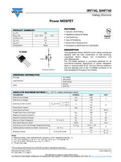
7 Maximum Current (Drain-to-Source) - What high current will melt the connections?Current vs. Gate-Source Voltage (Vgs) - What is the specific gain character?Gate Capacitance - The input Gate resistance is nearly infinite, but the Gate capacitance is substantial and often are tons more numbers, enough to fill four to ten pages with lists and charts and graphs for each type of device. International Rectifier seems to be the dominant supplier of power mosfets , and such information can be seen at their web site So what characteristics are important? Let s look at the data sheets of one of my favorites, the IRFP240, an N channel power transistor in a plastic off, it s rated at 200 Volts Drain-Source (that s good) and a maximum current of 20 amps (also good), and a maximum wattage dissipation of 150 watts (case temperature at 25 deg C. The maximum voltage between the Gate and Source is 20 Volts.)
8 These are important specs for selecting such a device, but you can pretty much figure that we aren t ordinarily going to be Testing them, as we are not usually looking to break the we go down the long list of numbers, some of interest for linear Audio stand out: Vgs, the threshold Gate voltage where conduction starts (anywhere from 2 to 5 Volts), the Transconductance (somewhere between 0 and 12, depending), and the Gate capacitance (anywhere from 1200 to 2400 pF, also depending). These figures vary with voltages, current, temperature, and also by device. (I would reproduce these figures and curves here, but we don t have that much space, and I d just as soon not have to deal with IR for permission). The transconductance is measured in Siemens, and is simply how many amps more flow from Drain to Source for each additional volt on the Gate-Source Gate capacitance is important, for while the input impedance looks close to infinity at DC, there is what looks to be a capacitor of quite a few picoFarads attached from Gate-Source and Gate-Drain, both of which start creating a load at high frequencies for whatever is trying to drive the Not is clear, however, that if you want to know what the performance will be for a given device in a circuit, you would best be measuring it yourself, not only because the manufacturer is not likely to be duplicating your exact circuit, but also because there is often wide variation between 4 Practical Mosfet Testing for AudioWhy match?
9 Often the reason for measuring Mosfet characteristics is to match devices to each other. Most often this consists of measuring the Vgs of the devices, and occasionally extends to measuring the the case of a power output stage, we often want to parallel power devices so as to share the current and heat dissipation, as in Figure 3a. Here it is desirable that the devices be identical so that the current is shared equally. If the Vgs of each device is different, some device will find itself doing the disproportionate share of the work while some other device might not be turned on at all. Even if the Vgs is matched at a given current for all devices, they might vary at different currents, so we either want to sample and match Vgs at different current and temperatures, or perhaps simply measure and match the transconductance at the operating point and cross our popular way around this is to match Vgs between devices having the same manufacturing lot code, meaning they were made at the same time under the same circumstances.
10 This technique is very effective, and if you sequentially measure the Vgs of a batch of smaller chips of the same lot code, you can actually visualize the position of the particular chip on the silicon wafer by the Vgs pattern that develops. These devices are usually extremely well matched in all other part of a typical amplifier circuit where matching is important is the circuit of Figure 3b, the input differential pair which compares the input signal to the amplifier s output signal and amplifies the difference. This is known as feedback. Matching of these parts allows for low DC offset at the amplifier output, good characteristic tracking over a range of temperatures, and (hopefully) lower distortion. I say hopefully because ideally you want the distortion characteristics of the matched pair to cancel exactly. You are well advised to not assume that matching will actually do is a key to performance in monolithic circuits such as op amps, where it can be conveniently assumed that transistors made next to each other will be very similar.