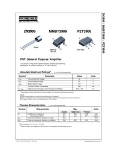
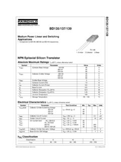
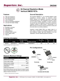
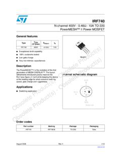
Transcription of TL082 Wide Bandwidth Dual JFET Input …
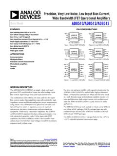
1 APRIL1998 REVISEDAPRIL2013TL082 WideBandwidthDualJFETI nputOperationalAmplifierCheckforSamples: TL082 -N1 FEATURESDESCRIPTIONT hesedevicesarelowcost,highspeed,dualJFET 23 InternallyTrimmedOffsetVoltage:15mVinput operationalamplifierswithaninternallytri mmed LowInputBiasCurrent:50pAinputoffsetvolta ge( BI-FETII technology).They LowInputNoiseVoltage:16nV/ Hzrequirelowsupplycurrentyetmaintaina ,well HzmatchedhighvoltageJFET inputdevicesprovide WideGainBandwidth:4 HighSlewRate:13V/ spincompatiblewiththestandardLM1558allow ingdesignerstoimmediatelyupgradetheovera ll HighInputImpedance:1012 designs. LowTotalHarmonicDistortion: applicationssuchas Low1/fNoiseCorner:50 Hzhighspeedintegrators,fastD/Aconverters ,sample.
2 2 sandholdcircuitsandmanyothercircuitsrequ iringlowinputoffsetvoltage,lowinputbiasc urrent,highinputimpedance, (TopView)SeePackageNumberD0008 AorP0008E1 Pleasebeawarethatanimportantnoticeconcer ningavailability,standardwarranty,anduse in is a 1998 2013, APRIL1998 (1)(2)SupplyVoltage 18 VPowerDissipation(3)(4)OperatingTemperat ureRange0 C to+70 CTj(MAX)150 CDifferentialInputVoltage 30 VInputVoltageRange(5) 15 VOutputShortCircuitDurationContinuousSto rageTemperatureRange 65 C to+150 CLeadTemp.(Soldering,10seconds)260 CESD ratingtobedetermined.(1) AbsoluteMaximumRatings functional,butdonotensurespecificperform ancelimits.
3 (2)If Military/Aerospacespecifieddevicesarereq uired,pleasecontacttheTexasInstrumentsSa lesOffice/Distributorsforavailabilityand specifications.(3)Thepowerdissipationlim it,however,cannotbeexceeded.(4)Foroperat ingatelevatedtemperature,thedevicemustbe deratedbasedona thermalresistanceof115 C/WjunctiontoambientfortheP0008 Epackage.(5)Unlessotherwisespecifiedthea bsolutemaximumnegativeinputvoltageis 1998 2013, APRIL1998 REVISEDAPRIL2013 DCElectricalCharacteristics(1) TL082 CSymbolParameterConditionsUnitsMinTypMax VOSI nputOffsetVoltageRS= 10k , TA= 25 C515mVOverTemperature20mV VOS/ TAverageTCofInputOffsetVoltageRS= 10k 10 V/ CIOSI nputOffsetCurrentTj= 25 C,(1)(2)25200pATj 70 C4nAIBI nputBiasCurrentTj= 25 C,(1)(2)
4 50400pATj 70 C8nARINI nputResistanceTj= 25 C1012 AVOLL argeSignalVoltageGainVS= 15V,TA= 25 C,25100V/mVVO= 10V,RL= 2 k OverTemperature15V/mVVOO utputVoltageSwingVS= 15V,RL= 10k 12 15V 11+15 VRange 12 VCMRRC ommon-ModeRejectionRatioRS 10k 70100dBPSRRS upplyVoltageRejectionRatio(3) (1)ThesespecificationsapplyforVS= 15 Vand0 C TA +70 , IBandIOSaremeasuredatVCM= 0.(2)Theinputbiascurrentsarejunctionleak agecurrentswhichapproximatelydoubleforev ery10 C increasein thejunctiontemperature,Tj. Duetothelimitedproductiontesttime, resultofinternalpowerdissipation,PD. Tj= TA+ jAPDwhere heatsinkis recommendedif inputbiascurrentis tobekepttoa minimum.
5 (3)Supplyvoltagerejectionratiois measuredforbothsupplymagnitudesincreasin gordecreasingsimultaneouslyin 6 Vto (1) TL082 CSymbolParameterConditionsUnitsMinTypMax AmplifiertoAmplifierCouplingTA= 25 C,f = 1Hz-20kHz 120dB(InputReferred)SRSlewRateVS= 15V,TA= 25 C813V/ sGBWGainBandwidthProductVS= 15V,TA= 25 C4 MHzenEquivalentInputNoiseVoltageTA= 25 C,RS= 100 ,25nV/ Hzf = 1000 HzinEquivalentInputNoiseCurrentTj= 25 C,f = HzTHDT otalHarmonicDistortionAV= +10,RL= 10k,< 20Vp p,BW= 20Hz 20kHz(1)ThesespecificationsapplyforVS= 15 Vand0 C TA +70 , IBandIOSaremeasuredatVCM= 1998 2013,TexasInstrumentsIncorporatedSubmitD ocumentationFeedback3 ProductFolderLinks: TL082 -NTL082-NSNOSBW5 C APRIL1998 1998 2013, APRIL1998 REVISEDAPRIL2013 TypicalPerformanceCharacteristics(contin ued) 1998 2013,TexasInstrumentsIncorporatedSubmitD ocumentationFeedback5 ProductFolderLinks.
6 TL082 -NTL082-NSNOSBW5C APRIL1998 (continued) 1998 2013, APRIL1998 REVISEDAPRIL2013 TypicalPerformanceCharacteristics(contin ued)OpenLoopVoltageGain(V/V) 1998 2013,TexasInstrumentsIncorporatedSubmitD ocumentationFeedback7 ProductFolderLinks: TL082 -NTL082-NSNOSBW5 C APRIL1998 1998 2013, APRIL1998 REVISEDAPRIL2013 PulseResponse(continued)CurrentLimit(RL= 100 ) 1998 2013,TexasInstrumentsIncorporatedSubmitD ocumentationFeedback9 ProductFolderLinks: TL082 -NTL082-NSNOSBW5 C APRIL1998 (BI-FETII). ,largedifferentialinputvoltagescaneasily beaccommodatedwithouta largeincreasein ,neitheroftheinputvoltagesshouldbeallowe dtoexceedthenegativesupplyasthiswillcaus elargecurrentstoflowwhichcanresultin a latchoccursinceraisingtheinputbackwithin thecommon-moderangeagainputstheinputstag eandthustheamplifierina singleinputwillnotchangethephaseoftheout put;however,ifbothinputsexceedthelimit,t heoutputoftheamplifierwillbeforcedtoa common-modeinputvoltageequaltothepositiv esupply.
7 However, ,anincreasein zenerreferencewhichallowsnormalcircuitop erationon 2 k loadresistanceto 10 Voverthefulltemperaturerangeof0 C to+70 theamplifieris forcedtodriveheavierloadcurrents,however , notinadvertentlyinstalledbackwardsin a socketasanunlimitedcurrentsurgethroughth eresultingforwarddiodewithintheICcouldca usefusingoftheinternalconductorsandresul tina ,careshouldbetakenwithleaddress, ,resistorsfromtheoutputtoaninputshouldbe placedwiththebodyclosetotheinputtominimi ze pick-up (usuallytheinvertinginput) ,if thefeedbackpoleislessthanapproximately6 timestheexpected3 dBfrequencya parallelsis 1998 2013, APRIL1998 REVISEDAPRIL2013 DetailedSchematicCopyright 1998 2013,TexasInstrumentsIncorporatedSubmitD ocumentationFeedback11 ProductFolderLinks: TL082 -NTL082-NSNOSBW5 C APRIL1998 Allpotentiometersarelineartaper , , , , 1998 2013, APRIL1998 REVISEDAPRIL2013andareseparateisolatedgr oundsMatchingofR2's, R4's andR5's controlCMRRWithAVT= 1400,resistormatching= :CMRR= 136dB Veryhighinputimpedance 1998 2013,TexasInstrumentsIncorporatedSubmitD ocumentationFeedback13 ProductFolderLinks.
8 TL082 -NTL082-NSNOSBW5C APRIL1998 1998 2013, APRIL1998 1998 2013,TexasInstrumentsIncorporatedSubmitD ocumentationFeedback15 ProductFolderLinks: TL082 -NTL082-NSNOSBW5 C APRIL1998 (April2013)toRevisionCPage 1998 2013,TexasInstrumentsIncorporatedProduct FolderLinks: TL082 -NPACKAGE OPTION 1 PACKAGING INFORMATIONO rderable DeviceStatus(1)Package TypePackageDrawingPinsPackageQtyEco Plan(2)Lead/Ball Finish(6)MSL Peak Temp(3)Op Temp ( C)Device Marking(4/5)SamplesTL082CM/NOPBACTIVESOI CD895 Green (RoHS& no Sb/Br)CU SNLevel-1-260C-UNLIM0 to 70TL082 CMTL082 CMXNRNDSOICD82500 TBDCall TICall TI0 to 70TL082 CMTL082 CMX/NOPBACTIVESOICD82500 Green (RoHS& no Sb/Br)CU SNLevel-1-260C-UNLIM0 to 70TL082 CMTL082CP/NOPBACTIVEPDIPP840 Green (RoHS& no Sb/Br)CU SNLevel-1-NA-UNLIM0 to 70TL082CP (1) The marketing status values are defined as follows:ACTIVE.
9 Product device recommended for new : TI has announced that the device will be discontinued, and a lifetime-buy period is in : Not recommended for new designs. Device is in production to support existing customers, but TI does not recommend using this part in a new : Device has been announced but is not in production. Samples may or may not be : TI has discontinued the production of the device. (2) Eco Plan - The planned eco-friendly classification: Pb-Free (RoHS), Pb-Free (RoHS Exempt), or Green (RoHS & no Sb/Br) - please check for the latest availabilityinformation and additional product content : The Pb-Free/Green conversion plan has not been (RoHS): TI's terms "Lead-Free" or "Pb-Free" mean semiconductor products that are compatible with the current RoHS requirements for all 6 substances, including the requirement thatlead not exceed by weight in homogeneous materials.
10 Where designed to be soldered at high temperatures, TI Pb-Free products are suitable for use in specified lead-free (RoHS Exempt): This component has a RoHS exemption for either 1) lead-based flip-chip solder bumps used between the die and package, or 2) lead-based die adhesive used betweenthe die and leadframe. The component is otherwise considered Pb-Free (RoHS compatible) as defined (RoHS & no Sb/Br): TI defines "Green" to mean Pb-Free (RoHS compatible), and free of Bromine (Br) and Antimony (Sb) based flame retardants (Br or Sb do not exceed by weightin homogeneous material) (3) MSL, Peak Temp.