Transcription of Transition-mode PFC controller
1 L6562. Transition-mode PFC controller . 1 Features Figure 1. Packages REALISED IN BCD TECHNOLOGY. Transition-mode CONTROL OF PFC PRE- REGULATORS. PROPRIETARY MULTIPLIER DESIGN FOR DIP-8 SO-8. MINIMUM THD OF AC INPUT CURRENT. VERY PRECISE ADJUSTABLE OUTPUT Table 1. Order Codes OVERVOLTAGE PROTECTION Part Number Package ultra -LOW ( 70 A) START-UP CURRENT L6562N DIP-8. LOW ( 4 mA) QUIESCENT CURRENT. L6562D SO-8. EXTENDED IC SUPPLY VOLTAGE RANGE. L6562 DTR Tape & Reel ON-CHIP FILTER ON CURRENT SENSE. DISABLE FUNCTION. DESKTOP PC, MONITOR) UP TO 300W. 1% (@ Tj = 25 C) INTERNAL REFERENCE. VOLTAGE HI-END AC-DC ADAPTER/CHARGER. -600/+800mA TOTEM POLE GATE DRIVER WITH ENTRY LEVEL SERVER & WEB SERVER.
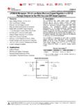
2 UVLO PULL-DOWN AND VOLTAGE CLAMP. 2 Description DIP-8/SO-8 PACKAGES ECOPACK . The L6562 is a current-mode PFC controller oper- APPLICATIONS ating in Transition Mode (TM). Pin-to-pin compati- PFC PRE-REGULATORS FOR: ble with the predecessor L6561, it offers improved IEC61000-3-2 COMPLIANT SMPS (TV, performance. Figure 2. Block Diagram COMP MULT CS. 2 3 4. 1. INV - MULTIPLIER AND 40K. THD OPTIMIZER. +. 5pF. VOLTAGE OVERVOLTAGE - +. REGULATOR DETECTION VCC. 8. VCC INTERNAL. SUPPLY 7V R Q 15 V. 25 V. S. R1 7. GD. + UVLO DRIVER. R2 - Starter VREF2. stop ZERO CURRENT. DETECTOR. +. V STARTER. V - DISABLE. 6 5. GND ZCD. Rev. 8. November 2005 1/16.)
3 L6562. 2 Description (continued). The highly linear multiplier includes a special circuit, able to reduce AC input current distortion, that allows wide-range-mains operation with an extremely low THD, even over a large load range. The output voltage is controlled by means of a voltage-mode error amplifier and a precise (1% @Tj =. 25 C) internal voltage reference. The device features extremely low consumption ( 70 A before start-up and <4 mA running) and includes a disable function suitable for IC remote ON/OFF, which makes it easier to comply with energy saving norms (Blue Angel, EnergyStar, Energy2000, etc.). An effective two-step OVP enables to safely handle overvoltages either occurring at start-up or resulting from load disconnection.
4 The totem-pole output stage, capable of 600 mA source and 800 mA sink current, is suitable for big MOS- FET or IGBT drive which, combined with the other features, makes the device an excellent low-cost solu- tion for EN61000-3-2 compliant SMPS's up to 300W. Table 2. Absolute Maximum Ratings Symbol Pin Parameter Value Unit VCC 8 IC Supply voltage (Icc = 20 mA) self-limited V. --- 1 to 4 Analog Inputs & Outputs to 8 V. IZCD 5 Zero Current Detector Max. Current -50 (source) mA. 10 (sink). Ptot Power Dissipation @Tamb = 50 C (DIP-8) 1 W. (SO-8) Tj Junction Temperature Operating range -40 to 150 C. Tstg Storage Temperature -55 to 150 C.
5 Figure 3. Pin Connection (Top view). INV 1 8 Vcc COMP 2 7 GD. MULT 3 6 GND. CS 4 5 ZCD. Table 3. Thermal Data Symbol Parameter SO8 Minidip Unit Rth j-amb Max. Thermal Resistance, Junction-to-ambient 150 100 C/W. 2/16. L6562. Table 4. Pin Description N Pin Function 1 INV Inverting input of the error amplifier. The information on the output voltage of the PFC pre- regulator is fed into the pin through a resistor divider. 2 COMP Output of the error amplifier. A compensation network is placed between this pin and INV (pin #1) to achieve stability of the voltage control loop and ensure high power factor and low THD. 3 MULT Main input to the multiplier.
6 This pin is connected to the rectified mains voltage via a resistor divider and provides the sinusoidal reference to the current loop. 4 CS Input to the PWM comparator. The current flowing in the MOSFET is sensed through a resistor, the resulting voltage is applied to this pin and compared with an internal sinusoidal-shaped reference, generated by the multiplier, to determine MOSFET's turn-off. 5 ZCD Boost inductor's demagnetization sensing input for Transition-mode operation. A negative-going edge triggers MOSFET's turn-on. 6 GND Ground. Current return for both the signal part of the IC and the gate driver. 7 GD Gate driver output.
7 The totem pole output stage is able to drive power MOSFET's and IGBT's with a peak current of 600 mA source and 800 mA sink. The high-level voltage of this pin is clamped at about 12V to avoid excessive gate voltages in case the pin is supplied with a high Vcc. 8 Vcc Supply Voltage of both the signal part of the IC and the gate driver. The supply voltage upper limit is extended to 22V min. to provide more headroom for supply voltage changes. Table 5. Electrical Characteristics (Tj = -25 to 125 C, VCC = 12, CO = 1 nF; unless otherwise specified). Symbol Parameter Test Condition Min. Typ. Max. Unit SUPPLY VOLTAGE. VCC Operating range After turn-on 22 V.
8 VCCon Turn-on threshold (1) 11 12 13 V. VCCOff Turn-off threshold (1) V. Hys Hysteresis V. VZ Zener Voltage ICC = 20 mA 22 25 28 V. SUPPLY CURRENT. Istart-up Start-up Current Before turn-on, VCC =11V 40 70 A. Iq Quiescent Current After turn-on mA. ICC Operating Supply Current @ 70 kHz 5 mA. Iq Quiescent Current During OVP (either static or mA. dynamic) or VZCD =150 mV. MULTIPLIER INPUT. IMULT Input Bias Current VVFF = 0 to 4 V -1 A. VMULT Linear Operation Range 0 to 3 V. V CS Output Max. Slope VMULT = 0 to V/V. --------------------- VCOMP = Upper clamp V MUL T. K Gain (2) VMULT = 1 V, VCOMP = 4 V 1/V. ERROR AMPLIFIER. VINV Voltage Feedback Input Tj = 25 C V.
9 Threshold (1) V < Vcc < 22 V. Line Regulation Vcc = V to 22V 2 5 mV. IINV Input Bias Current VINV = 0 to 3 V -1 A. 3/16. L6562. Table 5. Electrical Characteristics (continued). (Tj = -25 to 125 C, VCC = 12, CO = 1 nF; unless otherwise specified). Symbol Parameter Test Condition Min. Typ. Max. Unit Gv Voltage Gain Open loop 60 80 dB. GB Gain-Bandwidth Product 1 MHz ICOMP Source Current VCOMP = 4V, VINV = V -2 -5 mA. Sink Current VCOMP = 4V, VINV = V mA. VCOMP Upper Clamp Voltage ISOURCE = mA 6 V. Lower Clamp Voltage ISINK = mA (1) V. CURRENT SENSE COMPARATOR. ICS Input Bias Current VCS = 0 -1 A. td(H-L) Delay to Output 200 350 ns VCS clamp Current sense reference clamp VCOMP = Upper clamp V.
10 VCSoffset Current sense offset VMULT = 0 30 mV. VMULT = 5. ZERO CURRENT DETECTOR. VZCDH Upper Clamp Voltage IZCD = mA V. VZCDL Lower Clamp Voltage IZCD = mA 1 V. VZCDA Arming Voltage (3) V. (positive-going edge). VZCDT Triggering Voltage (3) V. (negative-going edge). IZCDb Input Bias Current VZCD = 1 to V 2 A. IZCDsrc Source Current Capability mA. IZCDsnk Sink Current Capability mA. VZCDdis Disable threshold 150 200 250 mV. VZCDen Restart threshold 350 mV. IZCDres Restart Current after Disable 30 75 A. STARTER. tSTART Start Timer period 75 130 300 s OUTPUT OVERVOLTAGE. IOVP Dynamic OVP triggering current 35 40 45 A. Hys Hysteresis (3) 30 A.