Transcription of Ultralow Power, Low Distortion, Fully Differential ADC ...
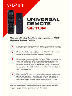
1 Ultralow Power, Low Distortion, Fully Differential ADC DriversData Sheet ada4940 -1/ ada4940 -2 Rev. D Document Feedback Information furnished by Analog Devices is believed to be accurate and reliable. However, no responsibility is assumed by Analog Devices for its use, nor for any infringements of patents or other rights of third parties that may result from its use. Specifications subject to change without notice. No license is granted by implication or otherwise under any patent or patent rights of Analog Devices.
2 Trademarks and registered trademarks are the property of their respective owners. One Technology Way, Box 9106, Norwood, MA 02062-9106, : 2011 2016 Analog Devices, Inc. All rights reserved. Technical Support FEATURES Small signal bandwidth: 260 MHz Ultralow power Extremely low harmonic distortion 122 dB THD at 50 kHz 96 dB THD at 1 MHz Low input voltage noise: nV/ Hz mV maximum offset voltage Balanced outputs Settling time to : 34 ns Rail-to-rail output: VS + V to +VS V Adjustable output common-mode voltage Flexible power supplies.
3 3 V to 7 V (LFCSP) Disable pin to reduce power consumption ada4940 -1 is available in LFCSP and SOIC packages APPLICATIONS Low power pulsar /SAR ADC drivers Single-ended-to- Differential conversion Differential buffers Line drivers Medical imaging Industrial process controls Portable electronics GENERAL DESCRIPTION The ada4940 -1/ ada4940 -2 are low noise, low distortion Fully Differential amplifiers with very low power consumption. They are an ideal choice for driving low power, high resolution, high performance SAR and - analog-to-digital converters (ADCs) with resolutions up to 16 bits from dc to 1 MHz on only mA of quiescent current.
4 The adjustable level of the output common-mode voltage allows the ada4940 -1/ ada4940 -2 to match the input common-mode voltage of multiple ADCs. The internal common-mode feedback loop provides exceptional output balance, as well as suppression of even-order harmonic distortion products. With the ada4940 -1/ ada4940 -2, Differential gain configurations are easily realized with a simple external feedback network of four resistors determining the closed-loop gain of the amplifier. The ada4940 -1/ ada4940 -2 are fabricated using Analog Devices, Inc.
5 , SiGe complementary bipolar process, enabling them to achieve very low levels of distortion with an input voltage noise of only nV/ Hz. The low dc offset and excellent dynamic performance of the ada4940 -1/ ada4940 -2 make them well suited for a variety of data acquisition and signal processing applications. FUNCTIONAL BLOCK DIAGRAMS NOTES1. CONNECT THE EXPOSED PAD TO VS OR FB+IN IN+FB OUTADA4940-1+OUTVOCM+VS+VS+VS+VS VS VS VS VS1211101349265781615141308452-001 Figure 1. ada4940 -1 IN1+FB1+VS1+VS1 FB2+IN2 IN2+FB2+VS2 VOCM2+OUT2+VS2 VS1 VS1 FB1+IN1 DISABLE1 OUT1 DISABLE1 VS2 VS2 VOCM1+OUT1 ada4940 -2 OUT207429-202213456181716151413891011712 201921222324 NOTES1.
6 CONNECT THE EXPOSED PAD TO VS OR GROUND. Figure 2. ada4940 -2 The ada4940 -1 is available in a 3 mm 3 mm, 16-lead LFCSP and an 8-lead SOIC. The ada4940 -2 is available in a 4 mm 4 mm, 24-lead LFCSP. The pinouts are optimized to facilitate printed circuit board (PCB) layout and minimize distortion. The ada4940 -1/ ada4940 -2 are specified to operate over the 40 C to +125 C temperature range. Table 1. Similar Products to ada4940 -1/ ada4940 -2 Product ISUPPLY (mA) Bandwidth (MHz) Slew Rate (V/ s) Noise (nV/ Hz) AD8137 3 110 450 ADA4932-1 9 560 2800 ADA4941-1 31 22 Table 2.
7 Complementary Products to ada4940 -1/ ada4940 -2 Product Power (mW) Throughput (MSPS) Resolution (Bits) SNR (dB) AD7982 1 18 98 AD7984 18 AD7621 65 3 16 88 AD7623 45 16 88 ada4940 -1/ ada4940 - 2 Data Sheet Rev.
8 D | Page 2 of 30 TABLE OF CONTENTS Features .. 1 Applications .. 1 General Description .. 1 Functional Block Diagrams .. 1 Revision History .. 3 Specifications .. 4 VS = 5 V .. 4 VS = 3 V .. 6 Absolute Maximum Ratings .. 8 Thermal Resistance .. 8 Maximum Power Dissipation .. 8 ESD Caution .. 8 Pin Configurations and Function Descriptions .. 9 Typical Performance Characteristics .. 11 Test Circuits .. 20 Terminology .. 21 Definition of Terms .. 21 Theory of Operation .. 22 Applications Information .. 23 Analyzing an Application Circuit.
9 23 Setting the Closed-Loop Gain .. 23 Estimating the Output Noise Voltage .. 23 Impact of Mismatches in the Feedback Networks .. 24 Calculating the Input Impedance of an Application Circuit 24 Input Common-Mode Voltage Range .. 25 Input and Output Capacitive AC Coupling .. 26 Setting the Output Common-Mode Voltage .. 26 DISABLE Pin .. 26 Driving a Capacitive Load .. 26 Driving a High Precision ADC .. 27 Layout, Grounding, and Bypassing .. 28 ada4940 -1 LFCSP Example .. 28 Outline Dimensions .. 29 Ordering Guide.
10 30 Data Sheet ada4940 -1/ ada4940 -2 Rev. D | Page 3 of 30 REVISION HISTORY 5/2016 Rev. C to Rev. D Changes to Figure 1 .. 1 Deleted Figure 1 Added Figure 2; Renumbered Sequentially .. 1 Updated Outline Dimensions .. 29 Changes to Ordering Guide .. 30 9/2013 Rev. B to Rev. C Updated Outline Dimensions .. 30 Changes to Ordering Guide .. 31 3/2012 Rev. A to Rev. B Reorganized Layout .. Universal Added ada4940 -1 8-Lead SOIC Package .. Universal Changes to Features Section, Table 1, and Figure 1; Replaced Figure 2.