Transcription of UNISONIC TECHNOLOGIES CO., LTD
1 UNISONIC TECHNOLOGIES CO., LTD LM321 LINEAR INTEGRATED CIRCUIT 1 of 7 Copyright 2017 UNISONIC TECHNOLOGIES Co., Ltd LOW POWER SINGLE OP AMP DESCRIPTION The UTC LM321 s quiescent current is only 430 A (5V). The UTC LM321 brings performance and economy to low power systems, With a high unity gain frequency and a specified s slew rate. The input common mode range includes ground and therefore the device is able to operate in single supply applications as well as in dual supply applications.
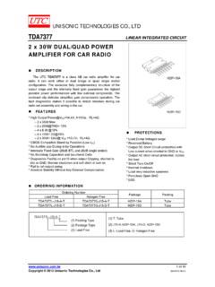
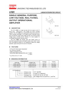
2 It is also capable of comfortably driving large capacitive loads. FEATURES * Low supply current 430 A * VCC=5V, TA=25 C. Typical values unless specified. * Gain-Bandwidth product 1 MHz * Low input bias current 45nA * Wide supply voltage range +3V~+32V * Stable with high capacitive loads ORDERING INFORMATION Ordering Number Lead Free Halogen Free Package Packing LM321L-AE5-R LM321G-AE5-R SOT-23-5 Tape Reel MARKING LM321 LINEAR INTEGRATED CIRCUIT UNISONIC TECHNOLOGIES CO.
3 , LTD 2 of 7 PIN CONFIGURATION PIN DESCRIPTION PIN NO. PIN NAME DESCRIPTION 1 +IN Non-inverting input 2 V- Ground 3 -IN inverting input 4 OUTPUT Output 5 V+ Power supply BLOCK DIAGRAM +INV--INV+OUTPUT+-45123 LM321 LINEAR INTEGRATED CIRCUIT UNISONIC
4 TECHNOLOGIES CO., LTD 3 of 7 ABSOLUTE MAXIMUM RATING PARAMETER SYMBOL RATINGS UNIT Supply Voltage (V+ - V ) VCC 32 V Differential Input Voltage VI(DIFF) Supply Voltage V Input Voltage VIN ~+32 V Input Current (VIN< ) (Note 2) 50 mA Output Short Circuit to GND, V+ 15V and TA=25 C (Note 3)
5 Continuous Junction Temperature TJ 150 C Storage Temperature TSTG -65~+150 C Notes: 1. Absolute maximum ratings are those values beyond which the device could be permanently damaged. Absolute maximum ratings are stress ratings only and functional device operation is not implied.
6 2. This input current will only exist when the voltage at any of the input leads is driven negative. It is due to the collector base junction of the input PNP transistors becoming forward biased and thereby acting as input diode clamps. In addition to this diode action, there is also lateral NPN parasitic transistor action on the IC chip. This transistor action can cause the output voltages of the op amps to go to the V+ voltage level (or to ground for a large overdrive) for the time duration that an input is driven negative.
7 This is not destructive and normal output states will re-establish when the input voltage, which was negative, again returns to a value greater than (at 25 C). 3. Short circuits from the output V+ can cause excessive heating and eventual destruction. When considering short circuits to ground the maximum output current is approximately 40mA independent of the magnitude of V+. At values of supply voltage in excess of +15V, continuous short circuits can exceed the power dissipation ratings and cause eventual destruction. OPERATING RATINGS PARAMETER SYMBOL RATINGS UNIT Temperature Range TA -40~85 C Supply Voltage V+ 3~30 V THERMAL DATA PARAMETER SYMBOL RATINGS
8 UNIT Junction to Ambient JA 265 С/W LM321 LINEAR INTEGRATED CIRCUIT UNISONIC TECHNOLOGIES CO., LTD 4 of 7 ELECTRICAL CHARACTERISTICS (Unless otherwise specified, all limits guaranteed for TA=25 C, V+=5V, V =0V, VO= ) PARAMETER SYMBOLTEST CONDITIONS MIN (Note 1) TYP (Note 2) MAX (Note 1)UNITI nput Offset Voltage VOS (Note 3) 2 7 mV Input Bias Current (Note 4)
9 IB 45 250 nA Input Offset Current IOS 5 50 nA Input Common-Mode Voltage Range VCM V+=30V (Note 5) For CMRR>=50dB 0 V+ 25 100 V/mVLarge Signal Voltage Gain AV (V+=15V, RL=2k VO= ~ ) 15 V/mVPower Supply Rejection Ratio PSRR RS 10k , V+ 5V~30V 65 100 dB Common Mode Rejection Ratio CMRR RS 10k 65 85 dB V+=30V.
10 RL=2k 26 V VOH V+=30V, RL=10k 27 28 V Output Swing VOL V+=5V, RL=10k 5 20 mV V+=5V mA Supply Current.