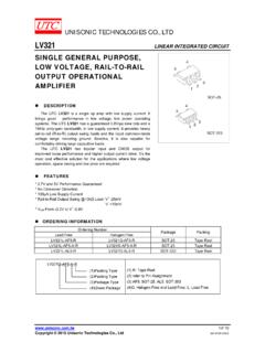
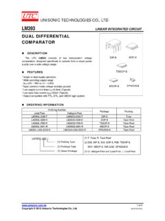
Transcription of UNISONIC TECHNOLOGIES CO., LTD
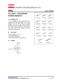
1 UNISONIC TECHNOLOGIES CO., LTD 16N50 Power MOSFET 1 of 7 Copyright 2019 UNISONIC TECHNOLOGIES Co., Ltd 16A, 500V N-CHANNEL POWER MOSFET DESCRIPTION The UTC 16N50 is a N-channel mode power MOSFET usingUTC s advanced technology to provide customers with planar stripe and DMOS technology. This technology allows a minimum on-state resistance and superior switching performance. It also can withstand high energy pulse in the avalanche and commutation mode. The UTC 16N50 is generally applied in high efficiency switch mode power supplies, active power factor correction and electronic lamp ballasts based on half bridge topology.
2 FEATURES * RDS(ON) @ VGS=10V, ID= * High Switching Speed * 100% Avalanche Tested SYMBOL TO-22011TO-220F1TO-220F21 ORDERING INFORMATION Ordering Number Pin Assignment Lead Free Halogen Free Package 1 2 3 Packing 16N50L-TA3-T 16N50G-TA3-T TO-220 G D S Tube 16N50L-TF1-T 16N50G-TF1-T TO-220F1 G D S Tube 16N50L-TF2-T 16N50G-TF2-T TO-220F2 G D S Tube Note.
3 Pin Assignment: G: Gate D: Drain S: Source 16N50G-TA3-T(1)Packing Type(2)Package Type(3)Green Package(1) T: Tube(2) TA3: TO-220, TF1: TO-220F1, TF2: TO-220F2(3) G: Halogen Free and Lead Free, L: Lead Free MARKING 16N50 Power MOSFET UNISONIC TECHNOLOGIES CO., LTD 2 of 7 ABSOLUTE MAXIMUM RATINGS (TC=25 С, unless otherwise specified) PARAMETER SYMBOL RATINGS UNIT Drain-Source Voltage VDSS 500 V Gate-Source Voltage VGSS 30 V Continuous ID 16 A Drain Current Pulsed (Note 2) IDM 64 A Avalanche Current (Note 2)
4 IAR A Avalanche Energy Single Pulsed (Note 3) EAS 832 mJ Peak Diode Recovery dv/dt (Note 4) dv/dt V/ns TO-220 220 W Power Dissipation TO-220F1/TO-220F2 PD 38 W Junction Temperature TJ +150 С Storage Temperature TSTG -55 ~ +150 С Notes: 1.
5 Absolute maximum ratings are those values beyond which the device could be permanently damaged. Absolute maximum ratings are stress ratings only and functional device operation is not implied. 2. Repetitive Rating : Pulse width limited by maximum junction temperature. 3. L=10mH, IAS= , VDD=50V, RG=25 , Starting TJ = 25 C 4. ISD 16A, di/dt 200A/ s, VDD BVDSS, Starting TJ = 25 C THERMAL DATA PARAMETER SYMBOL RATINGS UNIT Junction to Ambient JA C/W TO-220 C/W Junction to Case TO-220F1/TO-220F2 JC C/W 16N50
6 Power MOSFET UNISONIC TECHNOLOGIES CO., LTD 3 of 7 ELECTRICAL CHARACTERISTICS (TJ=25 C, unless otherwise specified) PARAMETER SYMBOLTEST CONDITIONS MIN TYP MAX UNITOFF CHARACTERISTICS Drain-Source Breakdown Voltage BVDSS ID=250 A, VGS=0V 500 V Drain-Source Leakage Current IDSS VDS=500V, VGS=0V 10 AForward VGS=+30V, VDS=0V +100 nAGate- Source Leakage Current Reverse IGSS VGS=-30V.
7 VDS=0V -100nAON CHARACTERISTICS Gate Threshold Voltage VGS(TH) VDS=VGS, ID=250 A Static Drain-Source On-State Resistance RDS(ON) VGS=10V, ID=8A DYNAMIC PARAMETERS Input Capacitance CISS 2330 pFOutput Capacitance COSS 260 pFReverse Transfer Capacitance CRSS VGS=0V, VDS=25V, f= 29 pFSWITCHING PARAMETERS Total Gate Charge (Note 1) QG 170 nCGate to Source Charge QGS 16 nCGate to Drain Charge QGD VDS=50V, VGS=10V, ID= , ID=100 A (Note 1, 2) nCTurn-ON Delay Time (Note 1) tD(ON) 114 nsRise Time tR 121 nsTurn-OFF Delay Time tD(OFF) 590 nsFall-Time tF VDS=30V, VGS=10V, ID= , RG=25 (Note 1, 2)
8 185 nsSOURCE- DRAIN DIODE RATINGS AND CHARACTERISTICS Maximum Body-Diode Continuous Current IS 16A Maximum Body-Diode Pulsed Current ISM 64A Drain-Source Diode Forward Voltage (Note 1)VSD IS=16A, VGS=0V Body Diode Reverse Recovery Time (Note 1) trr 375 nSBody Diode Reverse Recovery Charge Qrr IS=16A, VGS=0V, dIF/dt=100A/ s CNotes: 1. Pulse Test: Pulse width 300 s, Duty cycle 2%. 2. Essentially independent of operating ambient temperature. 16N50 Power MOSFET UNISONIC TECHNOLOGIES CO.
9 , LTD 4 of 7 TEST CIRCUITS AND WAVEFORMS Peak Diode Recovery dv/dt Test Circuit P. (Driver)ISD( )IFM, Body Diode Forward Currentdi/dtIRMBody Diode Reverse CurrentBody Diode Recovery dv/dtBody Diode Forward Voltage DropVDD10 VVDS( )VGS= Peak Diode Recovery dv/dt Waveforms 16N50 Power MOSFET UNISONIC TECHNOLOGIES CO., LTD 5 of 7 TEST CIRCUITS AND WAVEFORMS (Cont.) VDS90%10%VGStD(ON)tRtD(OFF)tFSwitching Test Circuit Switching Waveforms 10 VChargeQGSQGDQGVGSGate Charge Test Circuit Gate Charge Waveform VDDtpTimeBVDSSIASID(t)VDS(t) Unclamped Inductive Switching Test Circuit Unclamped Inductive Switching Waveforms 16N50 Power MOSFET UNISONIC TECHNOLOGIES CO.
10 , LTD 6 of 7 TYPICAL CHARACTERISTICS 16N50 Power MOSFET UNISONIC TECHNOLOGIES CO., LTD 7 of 7 UTC assumes no responsibility for equipment failures that result from using products at values that exceed, even momentarily, rated values (such as maximum ratings, operating condition ranges, or other parameters) listed in products specifications of any and all UTC products described or contained herein.