Transcription of Very High Common-Mode Voltage Precision Difference ...
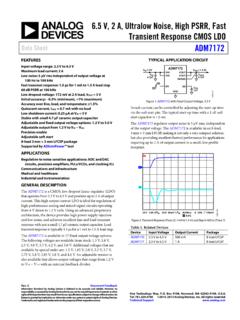
1 Very high Common-Mode Voltage Precision Difference Amplifier Data Sheet AD8479. FEATURES FUNCTIONAL BLOCK DIAGRAM. 600 V Common-Mode Voltage range AD8479. Rail-to-rail output REF( ) 1 8 NC. Fixed gain of 1. Wide power supply range of V to 18 V 7 +VS. 1M . 550 A typical power supply current IN 2. OUTPUT. Excellent ac specifications 6. +IN 3. 90 dB minimum CMRR 1M . 130 kHz bandwidth VS 4 5 REF(+). high accuracy dc performance 5 ppm maximum gain nonlinearity 11118-001. 10 V/ C maximum offset Voltage drift NOTES. 1. NC = NO CONNECT. DO NOT CONNECT TO THIS PIN.
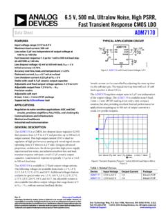
2 5 ppm/ C maximum gain drift Figure 1. APPLICATIONS. high Voltage current sensing Battery cell Voltage monitors Power supply current monitors Motor controls Isolation GENERAL DESCRIPTION. The AD8479 is a Difference amplifier with a very high input 800. Common-Mode Voltage range. The AD8479 is a Precision device 600. VS = 15V. that allows the user to accurately measure differential signals in Common-Mode Voltage (V). the presence of high Common-Mode voltages up to 600 V. 400. VS = 5V. The AD8479 can replace costly isolation amplifiers in applications 200.
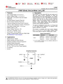
3 That do not require galvanic isolation. The device operates over 0. a 600 V Common-Mode Voltage range and has inputs that are protected from Common-Mode or differential mode transients 200. up to 600 V. 400. The AD8479 has low offset Voltage , low offset Voltage drift, 600. low gain drift, low Common-Mode rejection drift, and excellent Common-Mode rejection ratio (CMRR) over a wide frequency 800. 11118-110. 20 15 10 5 0 5 10 15 20. range. VOUT (V). The AD8479 is available in a space-saving 8-lead SOIC package Figure 2. Input Common-Mode Voltage vs.
4 Output Voltage and is operational over the 40 C to +125 C temperature range. Rev. A Document Feedback Information furnished by Analog Devices is believed to be accurate and reliable. However, no responsibility is assumed by Analog Devices for its use, nor for any infringements of patents or other rights of third parties that may result from its use. Specifications subject to change without notice. No One Technology Way, Box 9106, Norwood, MA 02062-9106, license is granted by implication or otherwise under any patent or patent rights of Analog Devices.
5 Tel: 2013 2015 Analog Devices, Inc. All rights reserved. Trademarks and registered trademarks are the property of their respective owners. Technical Support AD8479* PRODUCT PAGE QUICK LINKS. Last Content Update: 02/23/2017. COMPARABLE PARTS REFERENCE MATERIALS. View a parametric search of comparable parts. Press high Common-Mode Voltage Difference Amplifier EVALUATION KITS Enables Direct Interface to high Voltage Input up to 600. V. AD8479 Evaulation Board for the Precision Difference Amplifier DESIGN RESOURCES. DOCUMENTATION AD8479 Material Declaration Application Notes PCN-PDN Information AN-1308: Common-Mode Step Response of Current Sense Quality And Reliability Amplifiers Symbols and Footprints AN-1344: high Common-Mode Voltage Current Loop Transmitter Front End DISCUSSIONS.
6 AN-1375: Output Current Monitoring of high Voltage View all AD8479 EngineerZone Discussions. Class D Amplifiers Data Sheet SAMPLE AND BUY. AD8479: Very high Common-Mode Voltage Precision Visit the product page to see pricing options. Difference Amplifier Data Sheet Technical Books TECHNICAL SUPPORT. A Designer's Guide to Instrumentation Amplifiers, 3rd Edition, 2006 Submit a technical question or find your regional support number. User Guides AD8479: Evaluation Board for the Precision Difference DOCUMENT FEEDBACK. Amplifier (Wiki site). Submit feedback for this data sheet.
7 TOOLS AND SIMULATIONS. AD8479 SPICE Macro Model This page is dynamically generated by Analog Devices, Inc., and inserted into this data sheet. A dynamic change to the content on this page will not trigger a change to either the revision number or the content of the product data sheet. This dynamic page may be frequently modified. AD8479 Data Sheet TABLE OF CONTENTS. Features .. 1 Applications Information .. 12 Applications .. 1 Basic Connections .. 12 Functional Block Diagram .. 1 Single-Supply Operation .. 12 General Description .. 1 System-Level Decoupling and Grounding.
8 12 Revision History .. 2 Using a Large Shunt Resistor .. 13 3 Output Filtering .. 14 Absolute Maximum 4 Gain of 60 Differential Amplifier .. 14 ESD Caution .. 4 Error Budget Analysis Example .. 15 Pin Configuration and Function Descriptions .. 5 Outline Dimensions .. 16 Typical Performance Characteristics .. 6 Ordering Guide .. 16 Theory of Operation .. 11 REVISION HISTORY. 9/15 Rev. 0 to Rev. A. Changes to Single-Supply Operation Section .. 12. 4/13 Revision 0: Initial Version Rev. A | Page 2 of 16. Data Sheet AD8479. SPECIFICATIONS. VS = 15 V, REF( ) = REF(+) = 0 V, RL = 2 k , TA = 25 C, unless otherwise noted.
9 Table 1. A Grade B Grade Parameter Test Conditions/Comments Min Typ Max Min Typ Max Unit GAIN VOUT = 10 V, RL = 2 k . Nominal Gain 1 1 V/V. Gain Error %. Gain Nonlinearity 4 10 2 5 ppm Gain Drift TA = TMIN to TMAX 3 5 3 5 ppm/ C. OFFSET Voltage . Offset Voltage VS = 15 V 3 1 mV. VS = 5 V 3 1 mV. Offset Voltage Drift TA = TMIN to TMAX 3 15 3 10 V/ C. Power Supply Rejection VS = V to 15 V 84 100 90 100 dB. Ratio (PSRR). INPUT. Common-Mode Rejection VCM = 600 V dc Ratio (CMRR). TA = 25 C 80 90 90 96 dB. TA = TMIN to TMAX 80 90 dB. VCM = 1200 V p-p, dc to 12 kHz 80 80 dB.
10 Operating Voltage Range Common-Mode 600 600 V. Differential V. Input Operating Common-Mode 500 500 k . Impedance Differential 2 2 M . OUTPUT. Output Voltage Swing RL = 2 k VS + +VS VS + +VS V. Output Short-Circuit 55 55 mA. Current Capacitive Load Stable operation 500 500 pF. DYNAMIC RESPONSE. Small Signal 3 dB 130 130 kHz Bandwidth Slew Rate 8 8 V/ s Full Power Bandwidth VOUT = 20 V p-p 100 100 kHz Settling Time , VOUT = 10 V step 11 11 s , VCM = 10 V step s OUTPUT Voltage NOISE. Hz to 10 Hz 30 35 30 35 V p-p Noise Spectral Density f 100 Hz V/ Hz POWER SUPPLY.