Transcription of Voltage Output Temperature Sensor with Signal Conditioning ...
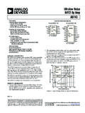
1 Voltage Output Temperature Sensor with Signal Conditioning AD22100. FEATURES FUNCTIONAL BLOCK DIAGRAM. V+. 200 C Temperature span Accuracy better than 2% of full scale Linearity better than 1% of full scale Temperature coefficient of mV/ C. Output proportional to Temperature V+ VOUT. Single-supply operation RT. 00673-C-001. Reverse Voltage protection Minimal self-heating High level, low impedance Output Figure 1. APPLICATIONS. HVAC systems +5V. System Temperature compensation Board level Temperature sensing REFERENCE. Electronic thermostats ANALOG-TO- DIGITAL.
2 MARKETS AD22100 Signal Output CONVERTER. VO DIRECT TO ADC. Industrial process control INPUT. 1k F. Instrumentation Automotive 50 C TO +150 C. 00673-C-002. GENERAL DESCRIPTION. The AD22100 is a monolithic Temperature Sensor with on-chip Figure 2. Application Circuit Signal Conditioning . It can be operated over the Temperature range 50 C to +150 C, making it ideal for use in numerous HVAC, instrumentation, and automotive applications. The Signal Conditioning eliminates the need for any trimming, buffering, or linearization circuitry, greatly simplifying the system design and reducing the overall system cost.
3 The Output Voltage is proportional to the Temperature x the supply Voltage (ratiometric). The Output swings from V at 50 C to + V at +150 C using a single + V supply. Due to its ratiometric nature, the AD22100 offers a cost- effective solution when interfacing to an analog-to-digital converter. This is accomplished by using the ADC's +5 V. power supply as a reference to both the ADC and the AD22100. eliminating the need for and cost of a precision reference (see Figure 2). Rev. D. Information furnished by Analog Devices is believed to be accurate and reliable.
4 However, no responsibility is assumed by Analog Devices for its use, nor for any infringements of patents or other rights of third parties that may result from its use. Specifications subject to change without notice. No license is granted by implication One Technology Way, Box 9106, Norwood, MA 02062-9106, or otherwise under any patent or patent rights of Analog Devices. Trademarks and Tel: registered trademarks are the property of their respective owners. Fax: 2004 Analog Devices, Inc. All rights reserved. AD22100. TABLE OF CONTENTS. 3 Output Stage Chip 3 Ratiometricity Considerations.
5 8. Absolute Maximum 4 Mounting Considerations ..8. ESD 4 Thermal Environment Effects ..8. Pin Configurations and Function Descriptions .. 5 Microprocessor A/D Interface Issues ..9. Typical Performance Characteristics .. 6 Use with a Precision Reference as the Supply Theory of Operation .. 7 Outline Dimensions .. 10. Absolute Accuracy and Nonlinearity Specifications .. 7 Ordering Guide .. 11. REVISION HISTORY. 7/04 Data Sheet Changed from Rev. C to Rev. D. Change to AD22100K 3. Updated Outline Dimensions .. 10. Changes to Ordering Guide .. 11. 6/04 Data Sheet Changed from Rev.
6 B to Rev. C. Changes to Format ..Universal Changes to Specifications .. 3. Changes to Chip Specifications .. 3. Changes to Ratiometricity Considerations Section .. 8. Changes to Ordering Guide .. 10. Updated Outline Dimensions .. 10. 12/94 Data Sheet Changed from Rev. A to Rev. B. Rev. D | Page 2 of 12. AD22100. SPECIFICATIONS. TA = 25 C and V+ = 4 V to V, unless otherwise noted. Table 1. AD22100K AD22100A AD22100S. Parameter Min Typ Max Min Typ Max Min Typ Max Unit TRANSFER FUNCTION VOUT = (V+/5 V) [ V +( mV/ C) TA] V. Temperature COEFFICIENT (V+/5 V) mV/ C.
7 TOTAL ERROR. Initial Error TA = 25 C C. Error Overtemperature TA = TMIN C. TA = TMAX C. Nonlinearity TA = TMAX to TMIN % FS1. Output CHARACTERISTICS. Nominal Output Voltage V+ = V, TA = 0 C V. V+ = V, TA = +100 C V. V+ = V, TA = 40 C V. V+ = V, TA = +85 C V. V+ = V, TA = 50 C V. V+ = V, TA = +150 C V. POWER SUPPLY. Operating Voltage V. Quiescent Current 500 650 500 650 500 650 A. Temperature RANGE. Guaranteed Temperature Range 0 +100 40 +85 50 +150 C. Operating Temperature Range 50 +150 50 +150 50 +150 C. PACKAGE TO-92 TO-92 TO-92. SOIC SOIC SOIC.
8 1. FS (full scale) is defined as the operating Temperature range 50 C to +150 C. The listed maximum specification limit applies to the guaranteed Temperature range. For example, the AD22100K has a nonlinearity of ( ) (200 C) = 1 C over the guaranteed Temperature range of 0 C to +100 C. CHIP SPECIFICATIONS. TA = 25 C and V+ = V, unless otherwise noted. Table 2. Paramater Min Typ Max Unit TRANSFER FUNCTION VOUT = (V+/5 V) [ V +( mV/ C) TA] V. Temperature COEFFICIENT (V+/5 V) mV/ C. Output CHARACTERISTICS. Error TA = 25 C C. Nominal Output Voltage TA = 25 C V.
9 POWER SUPPLY. Operating Voltage V. Quiescent Current 500 650 A. Temperature RANGE. Guaranteed Temperature Range +25 C. Operating Temperature Range 50 +150 C. Rev. D | Page 3 of 12. AD22100. ABSOLUTE MAXIMUM RATINGS. Table 3. Parameter Rating Supply Voltage 10 V Stresses above those listed under Absolute Maximum Ratings Reversed Continuous Supply Voltage 10 V may cause permanent damage to the device. This is a stress Operating Temperature 50 C to +150 C rating only and functional operation of the device at these or Storage Temperature 65 C to +160 C any other conditions above those indicated in the operational Output Short Circuit to V+ or Ground Indefinite section of this specification is not implied.
10 Exposure to absolute Lead Temperature Range 300 C maximum rating conditions for extended periods may affect (Soldering 10 sec) device reliability. Junction Temperature 150 C. ESD CAUTION. ESD (electrostatic discharge) sensitive device. Electrostatic charges as high as 4000 V readily accumulate on the human body and test equipment and can discharge without detection. Although this product features proprietary ESD protection circuitry, permanent damage may occur on devices subjected to high energy electrostatic discharges. Therefore, proper ESD precautions are recommended to avoid performance degradation or loss of functionality.
