Transcription of Zero-Drift, Digitally Programmable Sensor Signal …
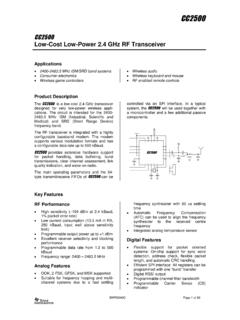
1 Zero- drift , Digitally Programmable Sensor Signal amplifier Data Sheet AD8555 FEATURES Very low offset voltage: 10 V maximum over temperature Very low input offset voltage drift : 60 nV/ C maximum High CMRR: 96 dB minimum Digitally Programmable gain and output offset voltage Single-wire serial interface Open and short wire fault detection Low-pass filtering Stable with any capacitive load Externally Programmable output clamp voltage for driving low voltage ADCs LFCSP-16 and SOIC-8 packages V to V operation 40 C to +125 C operation APPLICATIONS Pressure and position sensors Thermocouple amplifiers Industrial weigh scales Precision current sensing Strain gages FUNCTIONAL BLOCK DIAGRAM A3A2A4A5 VDDVDDDACVSSVSSVDDVSSVDDVDDVSSVCLAMPVPOS VSSFILT/DIGOUTVOUTA1 VDDVSSVNEGR1R3R2R5R7P4R4R6 RFP3P2P104598-0-001
2 Figure 1. GENERAL DESCRIPTION The AD8555 is a zero- drift , Sensor Signal amplifier with Digitally Programmable gain and output offset. Designed to easily and accurately convert variable pressure Sensor and strain bridge outputs to a well-defined output voltage range, the AD8555 also accurately amplifies many other differential or single-ended Sensor outputs. The AD8555 uses the ADI patented low noise auto-zero and DigiTrim technologies to create an incredibly accurate and flexible Signal processing solution in a very compact footprint. Gain is Digitally Programmable in a wide range from 70 to 1,280 through a serial data interface.
3 Gain adjustment can be fully simulated in-circuit and then permanently programmed with proven and reliable poly-fuse technology. Output offset voltage is also Digitally Programmable and is ratiometric to the supply voltage. In addition to extremely low input offset voltage and input offset voltage drift and very high dc and ac CMRR, the AD8555 also includes a pull-up current source at the input pins and a pull-down current source at the VCLAMP pin. This allows open wire and shorted wire fault detection. A low-pass filter function is implemented via a single low cost external capacitor. Output clamping set via an external reference voltage allows the AD8555 to drive lower voltage ADCs safely and accurately.
4 When used in conjunction with an ADC referenced to the same supply, the system accuracy becomes immune to normal supply voltage variations. Output offset voltage can be adjusted with a resolution of better than of the difference between VDD and VSS. A lockout trim after gain and offset adjustment further ensures field reliability. The AD8555 is fully specified over the extended industrial temperature range of 40 C to +125 C. Operating from single-supply voltages of V to V, t h e AD8555 is offered in the narrow 8-lead SOIC package and the 4 mm 4 mm 16-lead LFCSP. Rev. B Document Feedback Information furnished by Analog Devices is believed to be accurate and reliable.
5 However, no responsibility is assumed by Analog Devices for its use, nor for any infringements of patents or other rights of third parties that may result from its use. Specifications subject to change without notice. No license is granted by implication or otherwise under any patent or patent rights of Analog Devices. Trademarks and registered trademarks are the property of their respective owners. One Technology Way, Box 9106, Norwood, MA 02062-9106, Tel: 2004 2015 Analog Devices, Inc. All rights reserved. Technical Support AD8555 Data Sheet TABLE OF CONTENTS Features.
6 1 Applications .. 1 Functional Block Diagram .. 1 General Description .. 1 Revision History .. 2 Electrical Specifications .. 3 Absolute Maximum Ratings .. 7 ESD Caution .. 7 Pin Configurations and Function Descriptions .. 8 Typical Performance Characteristics .. 10 Theory of Operation .. 18 G a i n Va lues .. 19 Open Wire Fault Detection .. 20 Shorted Wire Fault Detection .. 20 Floating VPOS, VNEG, or VCLAMP Fault Detection .. 20 Device Programming .. 20 Filtering Function .. 26 Driving Capacitive Loads .. 26 RF Interference .. 27 Single-Supply Data Acquisition System .. 27 Using the AD8555 with Capacitive Sensors.
7 28 Outline Dimensions .. 29 Ordering Guide .. 29 REVISION HISTORY 2/15 Rev. A to Rev. B Changes to Applications Section .. 1 Changes to Table 5 .. 8 Changes to Figure 3 .. 9 Added Table 6; Renumbered Sequentially .. 9 Changes to Figure 64 .. 29 Updated Outline Dimensions .. 29 Changes to Ordering Guide .. 29 6/09 Rev. 0 to Rev A Changes to General Description .. 1 Changes to Figure 3 and Table 5 .. 8 Updated Outline Dimensions .. 28 Changes to Ordering Guide .. 28 4/04 Revision 0: Initial Version Rev. B | Page 2 of 29 Data Sheet AD8555 ELECTRICAL SPECIFICATIONS At VDD = V, VSS = V, VCM = V, VO = V, 40 C TA +125 C, unless otherwise specified.
8 Table 1. Parameter Symbol Conditions Min Typ Max Unit INPUT STAGE Input Offset Voltage VOS 2 10 V Input Offset Voltage drift TCVOS 25 65 nV/ C Input Bias Current IB TA = 25 C 12 16 22 nA 25 nA Input Offset Current IOS TA = 25 C 1 nA nA Input Voltage Range V Common-Mode Rejection Ratio CMRR VCM = V to V, AV = 70 80 92 dB VCM = V to V, AV = 1,280 96 112 dB Linearity VO = V to V 20 ppm VO = V to V 1000 ppm Differential Gain Accuracy Second Stage Gain = to 100 % Second Stage Gain = 140 to 200 % Differential Gain Temperature Coefficient Second Stage Gain = to 100 15 40 ppm/ C Second Stage Gain = 140 to 200 40 100 ppm/ C RF 14 18 22 k RF Temperature Coefficient 700 ppm/ C DAC Accuracy AV = 70, Offset Codes = 8 to 248 % Ratiometricity AV = 70, Offset Codes = 8 to 248 50 ppm Output Offset AV = 70.
9 Offset Codes = 8 to 248 5 35 mV Temperature Coefficient 15 ppm FS/ C VCLAMP Input Bias Current TA = 25 C, VCLAMP = 5 V 200 nA 500 nA Input Voltage Range V OUTPUT BUFFER STAGE Buffer Offset 7 15 mV Short-Circuit Current ISC 5 10 mA Output Voltage, Low VOL RL = 10 k to 5 V 30 mV Output Voltage, High VOH RL = 10 k to 0 V V POWER SUPPLY Supply Current ISY VO = V, VPOS = VNEG = , VDAC Code = 128 mA Power Supply Rejection Ratio PSRR AV = 70 109 125 dB DYNAMIC PERFORMANCE Gain Bandwidth Product GBP First Gain Stage, TA = 25 C 2 MHz Second Gain Stage, TA = 25 C 8 MHz Output Buffer Stage MHz Output Buffer Slew Rate SR AV = 70, RL = 10 k , C L = 100 pF V/ s Settling Time ts To , AV = 70, 4 V Output Step 8 s NOISE PERFORMANCE Input Referred Noise TA = 25 C, f = 1 kHz 32 nV/ Hz Low Frequency Noise en p-p f = Hz to 10 Hz V p-p Total Harmonic Distortion THD VIN = mV rms, f = 1 kHz, AV = 100 100 dB Rev.
10 B | Page 3 of 29 AD8555 Data Sheet Parameter Symbol Conditions Min Typ Max Unit DIGITAL INTERFACE Input Current 2 A DIGIN Pulse Width to Load 0 tw0 TA = 25 C 10 s DIGIN Pulse Width to Load 1 tw1 TA = 25 C 50 s Time between Pulses at DIGIN tws TA = 25 C 10 s DIGIN Low TA = 25 C 1 V DIGIN High TA = 25 C 4 V DIGOUT Logic 0 TA = 25 C 1 V DIGOUT Logic 1 TA = 25 C 4 V Rev. B | Page 4 of 29 Data Sheet AD8555 At VDD = V, VSS = V, VCM = V, VO = V, 40 C TA +125 C, unless otherwise specified. Table 2. Parameter Symbol Conditions Min Typ Max Unit INPUT STAGE Input Offset Voltage VOS 2 10 V Input Offset Voltage drift TCVOS 25 60 nV/ C Input Bias Current IB TA = 25 C 12 16 nA Input Offset Current IOS TA = 25 C 1 nA nA Input Voltage Range V Common-Mode Rejection Ratio CMRR VCM = V to V, AV = 70 80 92 dB VCM = V to V, AV = 1.