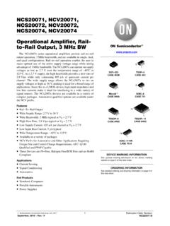
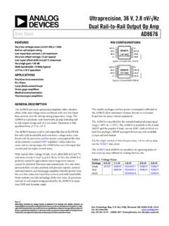
Transcription of Zero-Drift, Single-Supply, Rail-to-Rail Input/Output ...
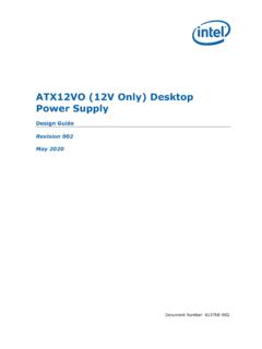
1 Zero-Drift, Single-Supply, Rail-to-Rail Input/Output Operational Amplifiers Data Sheet AD8551/AD8552/AD8554. FEATURES PIN CONFIGURATIONS. Low offset voltage: 1 V. NC 1 8 NC. Input offset drift: V/ C IN A V+. AD8551. Rail-to-Rail input and output swing +IN A OUT A. 01101-001. V 4 5 NC. 5 V single-supply operation NC = NO CONNECT. High gain, CMRR, PSRR: 130 dB Figure 1. 8-Lead MSOP (RM Suffix). Ultralow input bias current: 20 pA. Low supply current: 700 A/op amp NC 1 8 NC. Overload recovery time: 50 s IN A 2 7 V+. AD8551. No external capacitors required +IN A 3 6 OUT A. V 4 5 NC. APPLICATIONS. 01101-002.
2 NC = NO CONNECT. Temperature sensors Figure 2. 8-Lead SOIC (R Suffix). Pressure sensors Precision current sensing OUT A 1 8 V+. Strain gage amplifiers IN A OUT B. 01101-003. +IN A AD8552 IN B. Medical instrumentation V 4 5 +IN B. Thermocouple amplifiers Figure 3. 8-Lead TSSOP (RU Suffix). GENERAL DESCRIPTION. OUT A 1 8 V+. This family of amplifiers has ultralow offset, drift, and bias IN A 2 7 OUT B. current. The AD8551, AD8552, and AD8554 are single, dual, AD8552. +IN A 3 6 IN B. 01101-004. and quad amplifiers featuring Rail-to-Rail input and output swings. V 4 5 +IN B. All are guaranteed to operate from V to 5 V with a single supply.
3 Figure 4. 8-Lead SOIC (R Suffix). The AD8551/AD8552/AD8554 provide the benefits previously found only in expensive auto-zeroing or chopper-stabilized OUT A. IN A. 1 14 OUT D. IN D. amplifiers. Using Analog Devices, Inc. topology, these new +IN A. V+ AD8554. +IN D. V . zero-drift amplifiers combine low cost with high accuracy. No +IN B +IN C. 01101-005. IN B IN C. external capacitors are required. OUT B 7 8 OUT C. Figure 5. 14-Lead TSSOP (RU Suffix). With an offset voltage of only 1 V and drift of V/ C, the AD8551/AD8552/AD8554 are perfectly suited for applications in which error sources cannot be tolerated.
4 Temperature, OUT A 1 14 OUT D. position and pressure sensors, medical equipment, and strain IN A 2 13 IN D. gage amplifiers benefit greatly from nearly zero drift over their +IN A 3 12 +IN D. V+ 4. operating temperature range. The Rail-to-Rail input and output AD8554 11 V . +IN B 5 10 +IN C. swings provided by the AD8551/AD8552/AD8554 make both IN B 6 9 IN C. high-side and low-side sensing easy. 01101-006. OUT B 7 8 OUT C. The AD8551/AD8552/AD8554 are specified for the extended Figure 6. 14-Lead SOIC (R Suffix). industrial/automotive temperature range ( 40 C to +125 C). The AD8551 single amplifier is available in 8-lead MSOP and 8-lead narrow SOIC packages.
5 The AD8552 dual amplifier is available in 8-lead narrow SOIC and 8-lead TSSOP surface- mount packages. The AD8554 quad is available in 14-lead narrow SOIC and 14-lead TSSOP packages. Rev. F Document Feedback Information furnished by Analog Devices is believed to be accurate and reliable. However, no responsibility is assumed by Analog Devices for its use, nor for any infringements of patents or other rights of third parties that may result from its use. Specifications subject to change without notice. No One Technology Way, Box 9106, Norwood, MA 02062-9106, license is granted by implication or otherwise under any patent or patent rights of Analog Devices.
6 Tel: 1999 2015 Analog Devices, Inc. All rights reserved. Trademarks and registered trademarks are the property of their respective owners. Technical Support AD8551/AD8552/AD8554 Data Sheet TABLE OF CONTENTS. Features .. 1 1/f Noise Characteristics .. 16. Applications .. 1 Intermodulation Distortion .. 17. General Description .. 1 Broadband and External Resistor Noise Considerations .. 18. Pin Configurations .. 1 output Overdrive 18. Revision History .. 2 Input Overvoltage Protection .. 18. 3 output Phase Reversal .. 18. Electrical Characteristics .. 3 Capacitive Load Drive .. 19. Absolute Maximum 5 Power-Up Behavior.
7 19. Thermal Characteristics .. 5 Applications Information .. 20. ESD Caution .. 5 A 5 V Precision Strain Gage Circuit .. 20. Typical Performance Characteristics .. 6 3 V Instrumentation Amplifier .. 20. Functional Description .. 14 A High Accuracy Thermocouple Amplifier .. 21. Amplifier Architecture .. 14 Precision Current Meter .. 21. Basic Auto-Zero Amplifier Theory .. 14 Precision Voltage 21. High Gain, CMRR, PSRR .. 15 Outline Dimensions .. 22. Maximizing Performance Through Proper Layout .. 16 Ordering Guide .. 24. REVISION HISTORY. 6/15 Rev. E to Rev. F 3/07 Rev. B to Rev. C. Change to Input Voltage Parameter, Table 3.
8 5 Changes to Specifications Section ..3. 11/12 to Rev. E 2/07 Rev. A to Rev. B. Changes to Figure 68 .. 21 Updated Format .. Universal Updated Outline Dimensions (RM-8) .. 22 Changes to Figure 16. Changes to Ordering Guide .. 24 Deleted Spice Model Section .. 19. Deleted Figure 63, Renumbered Sequentially .. 19. 9/08 Rev. C to Rev. D Changes to Ordering Guide .. 24. Changes to Ordering Guide .. 23. 11/02 Rev. 0 to Rev. A. Edits to Figure 60 .. 16. Updated Outline Dimensions .. 20. Rev. F | Page 2 of 24. Data Sheet AD8551/AD8552/AD8554. SPECIFICATIONS. ELECTRICAL CHARACTERISTICS. VS = 5 V, VCM = V, VO = V, TA = 25 C, unless otherwise noted.
9 Table 1. Parameter Symbol Conditions Min Typ Max Unit INPUT CHARACTERISTICS. Offset Voltage VOS 1 5 V. 40 C TA +125 C 10 V. Input Bias Current IB 10 50 pA. AD8551/AD8554 40 C TA +125 C nA. AD8552 40 C TA +85 C 160 300 pA. AD8552 40 C TA +125 C 4 nA. Input Offset Current IOS 20 70 pA. AD8551/AD8554 40 C TA +125 C 150 200 pA. AD8552 40 C TA +85 C 30 150 pA. AD8552 40 C TA +125 C 150 400 pA. Input Voltage Range 0 5 V. Common-Mode Rejection Ratio CMRR VCM = 0 V to +5 V 120 140 dB. 40 C TA +125 C 115 130 dB. Large Signal Voltage Gain1 AVO RL = 10 k , VO = V to V 125 145 dB. 40 C TA +125 C 120 135 dB.
10 Offset Voltage Drift VOS/ T 40 C TA +125 C V/ C. output CHARACTERISTICS. output Voltage High VOH RL = 100 k to GND V. RL = 100 k to GND @ 40 C to +125 C V. RL = 10 k to GND V. RL = 10 k to GND @ 40 C to +125 C V. output Voltage Low VOL RL = 100 k to V+ 1 10 mV. RL = 100 k to V+ @ 40 C to +125 C 2 10 mV. RL = 10 k to V+ 10 30 mV. RL = 10 k to V+ @ 40 C to +125 C 15 30 mV. output Short-Circuit Limit Current ISC 25 50 mA. 40 C to +125 C 40 mA. output Current IO 30 mA. 40 C to +125 C 15 mA. POWER SUPPLY. Power Supply Rejection Ratio PSRR VS = V to V 120 130 dB. 40 C TA +125 C 115 130 dB. Supply Current/Amplifier ISY VO = 0 V 850 975 A.