
1. General description - NXP
the CANL driver is switched off and the RTL bias changes to the pull-up current source. Reception continues by switching to the single-wire mode via pins CANH or CANL. When failures 4 or 7 are removed, the recessive bus levels are restored. If the differential
Download 1. General description - NXP

Information
Domain:
Source:
Link to this page:
Documents from same domain

AN10441 Level shifting techniques in I2C-bus design
www.nxp.comDocument information AN10441 Level shifting techniques in I2C-bus design Rev. 01 — 18 June 2007 Application note Info Content Keywords I2C-bus, level shifting Abstract Logic level shifting may be required when interfacing legacy devices with

AN3234: Washing Machine Three-Phase AC …
www.nxp.comWashing Machine Three-Phase AC Induction Motor Drive, Rev. 0 Indirect Vector Control 4 Freescale Semiconductor If you are looking for more theory on the field ...

1. General description - nxp.com
www.nxp.com1. General description The TJA1044 is part of the Mantis family of high-speed CAN transceivers. It provides an interface between a Controller Area Network (CAN) protocol controller and the physical

PCA9570 Remote 4-bit general purpose outputs for 1 MHz …
www.nxp.com1. General description The PCA9570 is a CMOS device that provides 4 bits of General Purpose parallel Output (GPO) expansion in low voltage processor and handheld battery powered mobile

P82B96 Dual bidirectional bus buffer - nxp.com
www.nxp.com1. General description The P82B96 is a bipolar IC that creates a non-latching, bidirectional, logic interface between the normal I2C-bus and a range of other bus configurations.It can interface

S32K144 EVB Quick Start Guide - NXP Semiconductors
www.nxp.comJ14 SWD connector. 3 EXTERNAL USE S32K144 EVBFeatures: ... USB connector of the USB cable to micro-B port J7 on the S32K144EVB. ... Windows, Linux and Mac operating systems. Using the MSD Flash Programmer 1. Locate the .srec file of your project , file is under the

Three-Phase BLDC Motor Sensorless Control Using …
www.nxp.comThis document describes the design of a three-phase brushless DC motor (BLDC motor) drive based on Freescale’s MC56F8013 and MC56F8023 dedicated motor control device. Brushless DC motors are popular in a wide application area.

AN11443 BFU550XR ISM 433 MHz LNA design - nxp.com
www.nxp.comAN11443 BFU550XR ISM 433 MHz LNA design Rev. 1 — 23 January 2014 Application note . Document information Info Content Keywords BFU520, BFU530, BFU550 series, ISM-band, 433MHz 866MHz Abstract This document describes an ISM Frequency LNA design on BFU5xxXR Starter kit

DSP56156 16-Bit Digital Signal Processor - nxp.com
www.nxp.comThe DSP56156 is a general-purpose MPU-style Digital Signal Processor (DSP). On a single semi- conductor chip, the DSP56156 comprises a very efficient 16-bit digital signal processing core, pro-

SAA7706H Car radio Digital Signal Processor (DSP)
www.nxp.comCar radio Digital Signal Processor (DSP) SAA7706H This text is here in white to force landscape pages to be rotated correctly when browsing through the pdf in the Acrobat reader.This text is here in _white to force landscape pages to be rotated correctly when browsing through the pdf in the Acrobat reader.This text is here inThis text is here in
Related documents
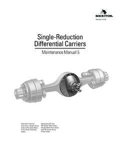
Single-Reduction Differential Carriers - Parts Manuals
partsmanuals.orgDifferential Carriers Maintenance Manual 5 Revised 10-06 Standard Carriers Including: Single Axles, Rear of Tandem Axles, Front Drive Steering Axles Excluding RS and RT Series (Rear Only), ... Driver-Controlled Full Locking Main Differential T-9007V. $50. Order T …

MAX3483/MAX3485/MAX3486/MAX3488/MAX3490/MAX3491 …
datasheets.maximintegrated.comDifferential Driver Output VOD RL = 100Ω (RS-422), Figure 4 2.0 RL = 54Ω (RS-485), Figure 4 1.5 V RL = 60Ω (RS-485), VCC = 3.3V, Figure 5 1.5 Change in Magnitude of Driver Differential Output Voltage for Complementary Output States (Note 1) ΔVOD RL = 54Ω or 100Ω, Figure 4 0.2 V Driver Common-Mode Output Voltage VOC RL = 54Ω or 100Ω ...

Board Design Guidelines for PCI Express™ Architecture
e2e.ti.com§Clock driver requirements: ü100MHz with SSC support (e.g. CK410) üSystem board (source) termination only üRise/fall slew rate requirements need to be met System board requirements L1 L1' L2 L2' L3' L3 L5 L5' Rs Rs Rt Rt PCI Express 1” Connector Clock Driver PCI Express Card L4 L4' 0.5” max 0–0.2” 0 – 0.2” – 14” 0.5” – 3 ...
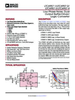
LTC6957-1/LTC6957-2/LTC6957-3/LTC6957-4 - Analog Devices
www.analog.comVINDIFF Input Signal Level Range, Differential l 0.2 0.8 2 VP-P tMIN Minimum Input Pulse Width High or Low 0.5 ns VINCM Self-Bias Voltage, IN+, IN– l 1.8 2 2.3 V RIN Input Resistance, Differential l 1.5 2 2.5 kΩ CIN Input Capacitance, Differential 0.5 pF BWIN ++ + LTC6957-2

AD8129/AD8130 Low Cost 270 MHz Differential Receiver ...
www.analog.commode and differential-mode voltage ranges while maintaining signal integrity. The wide common-mode voltage range enables the driver-receiver pair to operate without isolation transformers in many systems where the ground potential difference between drive and receive locations is many volts. The AD8129/AD8130
LM358 - Diodes Incorporated
www.diodes.comDifferential Input Voltage 32 V V IN Input Voltage -0.3 to +32 V P D Power Dissipation (Note 2) 600 mW Output Short-Circuit to GND (One Amplifier) (Note 3) V+ < 15V and T A=25 oC Continuous Input Current (V IN < -0.3V) (Note 4) 40 mA T OP Operating Temperature Range 0 to +70 oC T ST Storage Temperature Range -65 to +150 oC Notes: 2.
LM2596 - 3.0 A, Step-Down Switching Regulator
www.onsemi.comINPUT - OUTPUT DIFFERENTIAL (V) TJ, JUNCTION TEMPERATURE (°C) Figure 2. Normalized Output Voltage TJ, JUNCTION TEMPERATURE (°C) Figure 3. Line Regulation Figure 4. Dropout Voltage Figure 5. Current Limit Figure 6. Quiescent Current Figure 7. Standby Quiescent Current ILoad = 200 mA ILoad = 3.0 A Vin = 12 V Vin = 40 V L1 = 33 H Rind = 0.1 ...