Bipolar Transistor
speed than PNP transistors because the electron mobility is larger than the hole mobility. BJTs are almost exclusively of the NPN type since high performance is BJTs’ competitive edge over MOSFETs. Figure 8–1b shows that when the base–emitter junction is forward biased, electrons are injected into the more lightly doped base.
Download Bipolar Transistor

Information
Domain:
Source:
Link to this page:
Documents from same domain
MOS Transistor - Chenming Hu
www.chu.berkeley.eduModern MOSFET technology has advanced continually since its beginning in the 1950s. Figure 6–5 is a transmission electron microscope view of a part of a MOSFET. It shows the poly-Si gate and the single-crystalline Si body with visible individual Si atoms and a 1.2 nm amorphous SiO 2 film between them. 1.2 nm is the size of four SiO 2 molecules.

Device Fabrication Technology1 - Chenming Hu
www.chu.berkeley.edustarting material. A large wafer fab can process 40,000 silicon wafers into circuits each month. The simple example of the device fabrication process shown in Fig. 3–1 includes (a) formation of an SiO 2 layer, (b) its selective removal, (c) introduction of dopant atoms into the wafer surface, and (d) dopant diffusion into silicon. VLSI! ULSI!
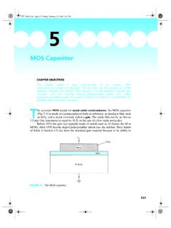
MOS Capacitor - Chenming Hu
www.chu.berkeley.edu1.5 nm. One nanometer is equal to 10 Å, or the size of a few oxide molecules. Before 1970, the gate was typically made of metals such as Al (hence the M in MOS). After 1970, heavily doped polycrystalline silicon (see the sidebar, Three Kinds of Solid, in Section 3.7) has been the standard gate material because of its ability to

MOSFETs in ICs—Scaling, Leakage, and Other Topics
www.chu.berkeley.eduThe electron and hole mobility can be raised (or lowered) by carefully engineered mechanical strains. The strain changes the lattice constant of the silicon crystal and therefore the E–k relationship through the Schrodinger’s wave equation. The E–k relationship, in turn, determines the effective mass and the mobility.
Electrons and Holes in Semiconductors
www.chu.berkeley.eduevery silicon atom has four other silicon atoms as its nearest neighbor atoms. This fact is illustrated in Fig. 1–2 with the darkened cluster of a center atom having four neighboring atoms. This cluster is called the primitive cell. Silicon is a group IV element in the periodic table and has four valence electrons. These four electrons
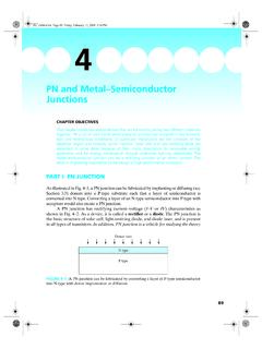
PN and Metal–Semiconductor Junctions
www.chu.berkeley.edu4.1 Building Blocks of the PN Junction Theory 93 (4.1.2) The built-in potential is determined by N a and N d through Eq. (4.1.2). The larger the N a or N d is, the larger the φbi is.Typically, φbi is about 0.9 V for a silicon PN junction. Since a lower E c means a higher voltage (see Section 2.4), the N side is at a higher voltage or electrical potential than the P side.
Motion and Recombination of Electrons and Holes
www.chu.berkeley.educollisions is typically 10–13s or 0.1 ps (picosecond), and the distance between collisions is a few tens of nanometers or a few hundred angstroms. The net thermal velocity (averaged over time or over a large number of carriers at any given time) is zero. Thus, thermal motion does not create a steady electric current, but it does introduce a
Related documents
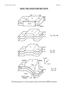
MOS TRANSISTOR REVIEW - Stanford University
web.stanford.eduFor small gate bias at high drain bias a significant drain leakage can be observed, especially for short channel devices. The electric field can be very high in the drain region for VD high and VG = 0. This can cause band-to-band tunneling. This will happen only if the electric field is sufficiently high to cause large band bending.

Lecture 12 Physical Vapor Deposition: Evaporation and ...
alan.ece.gatech.eduElectron momentum transfer to the ions in high current density lines. Solution: Add a small number (typically <3-5%) larger atoms such as copper that “anchor” the aluminum atoms in place or replace the entire metal line with larger atoms such as copper so that each atom is more difficult to move.

3. Short Channel Effects on MOS Transistors.
csit-sun.pub.ro• The electron velocity is related to the electric field through the mobility: (3) • Combining (1) and (3) in (2): I Ddx=µ nC OXW(V GS-V(x)-V T)dV (4) • Integrating (4) from 0 to L yields the voltage-current relation of the transistor: (5) • The behavior of the short channel devices deviates considerably from this model. • Eq.
Chapter 2 MOS Transistor Theory - NCU
www.ee.ncu.edu.twMOS transistors conduct electrical current by using ... ds than expected at high V ds Mobility degradation At high vertical field strengths (V gs/t ox), ... the electron speed will be high enough to break the electron-hole pair. Moreover, the electrons …
MOSFETs in ICs—Scaling, Leakage, and Other Topics
www.chu.berkeley.eduThe electron and hole mobility can be raised (or lowered) by carefully engineered mechanical strains. The strain changes the lattice constant of the silicon crystal and therefore the E–k relationship through the Schrodinger’s wave equation. The E–k relationship, in turn, determines the effective mass and the mobility.