Transcription of Chapter 2 MOS Transistor Theory - NCU
1 Chapter 2 MOS Transistor TheoryJin-Fu LiAdvanced Reliable Systems (ARES) of Electrical EngineeringNational Central UniversityJhongli, TaiwanAdvanced Reliable Systems (ARES) Lab. Jin-Fu Li, EE, NCU2 Introduction I-V Characteristics of MOS Transistors Nonideal I-V Effects Pass Transistor SummaryOutlineAdvanced Reliable Systems (ARES) Lab. Jin-Fu Li, EE, NCU3 MOS Transistor MOS transistors conduct electrical current by using an applied voltage to move charge from the sourceside to the drainside of the device An MOS Transistor is a majority-carrier device In an n-typeMOS Transistor , the majority carriers are electrons In a p-typeMOS Transistor , the majority carriers are holes Threshold voltage It is defined as the voltage at which an MOS device begins to conduct ( turn on ) MOS Transistor symbolsNMOSPMOSA dvanced Reliable Systems (ARES) Lab.
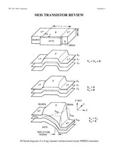
2 Jin-Fu Li, EE, NCU4 MOS Transistor So far, we have treated transistors as ideal switches An ON Transistor passes a finite amount of current Depends on terminal voltages Derive current-voltage (I-V) relationships Transistor gate, source, drain all have capacitance I = C ( V/ t) -> t = (C/I) V Capacitance and current determine speed The structure of a MOS Transistor is symmetric Terminals of source and drain of a MOS can be exchangedAdvanced Reliable Systems (ARES) Lab. Jin-Fu Li, EE, NCU5Vg& Channel for P-Type BodyVg<0 Accumulation mode0<Vg<VtVg>VtDepletion modeInversion modePolysilicon GateSilicon Dioxide InsulatorP-type BodyDepletion RegionInversion RegionDepletion RegionAdvanced Reliable Systems (ARES) Lab.
3 Jin-Fu Li, EE, NCU6 NMOS Transistor in Cutoff Moden+n+p-type bodyVgs=0 Vgdsdg Cutoff region The source and drain have free electrons The body has free holes but no free electrons The junction between the body and the source or drain are reverse-biased, so almost zero current flowsAdvanced Reliable Systems (ARES) Lab. Jin-Fu Li, EE, NCU7 NMOS Transistor in Linear ModeVgs>VtVgd=Vgsp-type bodysdgp-type bodysdgn+n+n+n+Vgs>Vgd>VtVgs>VtVds=00<Vds<Vgs-VtIds Linear region resistive, nonsaturated, or unsaturated region If Vgd=Vgs, then Vds=Vgs-Vgd=0 and there is no electrical field tending to push current from drain to source If Vgs>Vgd>Vt, then 0<Vds<Vgs-Vtand there is a small positive potential Vdsis applied to the drain.
4 Current Idsflows through the channel from drain to source The current increases with both the drain and gate voltageAdvanced Reliable Systems (ARES) Lab. Jin-Fu Li, EE, NCU8 NMOS Transistor in Saturation Modep-type bodysdgn+n+Vgd<VtVgs>VtVds>Vgs-Vt Saturation region The Vds becomes sufficiently large that Vgd<Vt, the channel is no longer inverted near the drain and becomes pinched off However, conduction is still brought about by the drift of electrons under the influence of the positive drain voltage As electrons reach the end of the channel, they are injected into the depletion region near the drain and accelerated toward the drain The current Ids is controlled by the gate voltage and ceases to be influenced by the drainIdsAdvanced Reliable Systems (ARES) Lab.
5 Jin-Fu Li, EE, NCU9 NMOS Transistor In summary, the NMOS Transistor has three modes of operations If Vgs<Vt, the Transistor is cutoff and no current flows If Vgs>Vt and Vdsis small, the Transistor acts as a linear resistor in which the current flow is proportional to Vds If Vgs>Vt and Vdsis large, the Transistor acts as a current source in which the current flow becomes independent of Vds The PMOS Transistor operates in just the opposite fashion Advanced Reliable Systems (ARES) Lab. Jin-Fu Li, EE, NCU10I-V Characteristics of MOS In linear and saturation regions, the gate attracts carriers to form a channel The carriers drift from source to drain at a rate proportional to the electric field between these regions MOS structure looks like parallel plate capacitor while operating in inversion Gate oxide channelN+N+VgAdvanced Reliable Systems (ARES) Lab.
6 Jin-Fu Li, EE, NCU11 Channel Charge Qchannel=Cg(Vgc-Vt) , where Cg is the capacitance of the gate to the channel and Vgc-Vtis the amount of voltage attracting charge to the channel beyond the minimal required to invert from p to n Vc=(Vs+Vd)/2=Vs+Vds/2 Therefore, Vgc=(Vgs+Vgd)/2=Vgs-Vds/2n+n+VgCgVsVdVcA dvanced Reliable Systems (ARES) Lab. Jin-Fu Li, EE, NCU12 Gate Capacitance (Cg) Transistor dimensions The gate capacitance is N+N+WLtOXGateoxoxgtWLC Advanced Reliable Systems (ARES) Lab. Jin-Fu Li, EE, NCU13 Carrier Velocity Charge is carried by e- Carrier velocity vproportional to lateral E-field between source and drain v= E, where is called mobility E = Vds/L Time for carrier to cross channel: t= L / vAdvanced Reliable Systems (ARES) Lab.
7 Jin-Fu Li, EE, NCU14 NMOS Linear I-V Now we know How much charge Qchannelis in the channel How much time teach carrier takes to cross Where channelox22dsdsgstdsdsgstdsQItWVCVV VLVVVV ox = WCL Advanced Reliable Systems (ARES) Lab. Jin-Fu Li, EE, NCU15 NMOS Saturation I-V If Vgd<Vt, channel pinches off near drain When Vds>Vdsat= Vgs Vt Now drain voltage no longer increases current 222dsatdsgstdsatgstVIVVVVV Advanced Reliable Systems (ARES) Lab. Jin-Fu Li, EE, NCU16 Summary of NMOS I-V Characteristics 2cutofflinearsaturatio022ngstdsdsgstdsds dsatgstdsdsatVVVIVV VVVVVVV (mA)Vgs = 5 Vgs = 4 Vgs = 3 Vgs = 2 Vgs = 1 Vds=Vgs-VtLinearSaturationAdvanced Reliable Systems (ARES) Lab.
8 Jin-Fu Li, EE, NCU17 Example Assume that the parameters of a technology are as follows tox= 100 = 350 cm2/V*s Vt= V Plot Idsvs. Vds Vgs= 0, 1, 2, 3, 4, 5 Use W/L = 4/2 (mA)Vgs = 5 Vgs = 4 Vgs = 3 Vgs = 2 Vgs = 128142 Advanced Reliable Systems (ARES) Lab. Jin-Fu Li, EE, NCU18 Nonideal I-V Effects Nonideal I-V effects Velocity saturation, mobility degradation, channel length modulation, subthreshold conduction, body effect, etc. The saturation current increases less than quadratically with increasing Vgs. This is caused by two effects: Velocity saturation mobility degradation Velocity saturation At high lateral field strengths (Vds/L), carrier velocity ceases to increase linearly with field strength Result in lower Idsthan expected at high Vds mobility degradation At high vertical field strengths (Vgs/tox), the carriers scatter more often Also lead to less current than expected at high VgsAdvanced Reliable Systems (ARES) Lab.
9 Jin-Fu Li, EE, NCU19 Ideally, Idsis independent of Vdsfor a Transistor in saturation, making the Transistor a perfect current source Actually, the width Ldof the depletion region between the channel and drain is increased with Vdb. To avoid introducing the body voltage into our calculations, assume the source voltage is close to the body voltage so Vdb~Vds Thus the effective channel length is shorten to Leff=L-Ld Therefore, the Ids can be expressed as Assume that , then Channel Length Modulation2)(21tgsoxdsVVCLWI LLVVCLWVVCLWI dtgsoxtgsoxeffds 11)(21)(2122 2211()(1)()(1)22ddsoxgstoxgstdsLWWICV VCV VVLLL 1 LLdAdvanced Reliable Systems (ARES) Lab.
10 Jin-Fu Li, EE, NCU20 The parameter is an empirical channel length modulation factor As channel length gets shorter, the effect of the channel length modulation becomes relatively more important Hence is inversely dependent on channel length This channel length modulation model is a gross oversimplification of nonlinear behavior and is more useful for conceptual understanding than for accurate device modeling Channel length modulation is very important to analog designers because it reduces the gain of amplifiers. It is generally unimportant for qualitatively understanding the behavior of digital circuitsChannel Length Modulation Advanced Reliable Systems (ARES) Lab.
![Training Course of Design Compiler [相容模式]](/cache/preview/c/f/6/f/4/1/7/2/thumb-cf6f4172c80a30be0667109e5a50ce98.jpg)
![hspice tutorial.ppt [相容模式] - ee.ncu.edu.tw](/cache/preview/0/1/e/d/5/5/6/4/thumb-01ed55640fe3958cfb144af3846e1fcf.jpg)