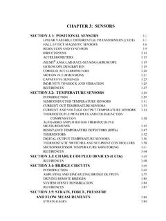
CHAPTER 3: SENSORS - Analog Devices
that signal conditioning circuits can be integrated on the same chip as the sensor. CMOS processes are common for this application. A simple rotational speed detector can be made with a Hall sensor, a gain stage, and a comparator as shown in Figure 3.8. The circuit is designed to detect rotation speed as in automotive applications. It responds to
Download CHAPTER 3: SENSORS - Analog Devices

Information
Domain:
Source:
Link to this page:
Documents from same domain

AD743 Ultralow Noise BiFET Op Amp Data Sheet …
www.analog.comREV. E Information furnished by Analog Devices is believed to be accurate and reliable. However, no responsibility is assumed by Analog Devices for its

MT-070: In-Amp Input RFI Protection - Analog …
www.analog.comRev.0, 10/08, WK Page 1 of 6 MT-070 TUTORIAL In-Amp Input RFI Protection . PROTECTING IN-AMPS AGAINST RFI . Real-world applications must deal with an ever increasing amount of radio frequency

LTC3108 - Ultralow Voltage Step-Up Converter and …
www.analog.comLTC3108 3108fc For more information www.linear.com/LTC3108 LDO

1.8 V Low Power CMOS Rail-to-Rail Input/Output …
www.analog.com1.8 V Low Power CMOS Rail-to-Rail Input/Output Operational Amplifier Data Sheet AD8515 Rev. E Document Feedback Information furnished by Analog Devices is believed to be accurate and reliable.

Low Cost Micropower, Low Noise CMOS Rail-to …
www.analog.comLow Cost Micropower, Low Noise CMOS Rail-to-Rail, Input/Output Operational Amplifiers Data Sheet AD8613/AD8617/AD8619 Rev. H Document Feedback Information furnished by Analog Devices is believed to be accurate and reliable.

Low Cost CMOS, High Speed, Rail-to-Rail Amplifiers
www.analog.comLow Cost CMOS, High Speed, Rail-to-Rail Amplifiers Data Sheet ADA4891-1/ADA4891-2/ADA4891-3/ADA4891-4 Rev. F Document Feedback Information furnished by Analog Devices ...

Zero-Drift, Single-Supply, Rail-to-Rail Input/Output ...
www.analog.comZero-Drift, Single-Supply, Rail-to-Rail Input/Output Operational Amplifier Data Sheet AD8628/AD8629/AD8630 FEATURES Lowest auto-zero amplifier noise Low offset voltage: 1 µV AD8628

FEATURES DESCRIPTIO U - analog.com
www.analog.com1 LT1025 1025fb DESCRIPTIO U APPLICATIO S U 80µA Supply Current 4V to 36V Operation 0.5°C Initial Accuracy (A Version) Compatible with Standard Thermocouples (E, J, K, R, S, T) Auxiliary 10mV/°C Output Available in 8-Lead PDIP and SO Packages Thermocouple Cold Junction Compensator Centigrade Thermometer Temperature …

LT1173 - Micropower DC/DC Converter Adjustable …
www.analog.comLT1173 1 Micropower DC/DC Converter Adjustable and Fixed 5V, 12V VOUT 5V/DIV 0V PROGRAM 5V/DIV 5ms/DIV 1173 TA02 L1* 100µH LT1173 • TA01 + GND SW2 FB SW1 ILIM VIN 10 F LT1173

AD9850 CMOS, 125 MHz Complete DDS …
www.analog.comrev. h a cmos, 125 mhz complete dds synthesizer ad9850 functional block diagram clock out clock out analog in analog out dac rset …
Related documents

Introduction to Switched-Capacitor Circuits
www.seas.ucla.eduChapter 12. Introduction to Switched-Capacitor Circuits 397 t Vin Vout Figure 12.3. Step response of the amplifier of Fig. 12.2(b). step. Illustrated in Fig. 12.3, the response contains a step change due to the initial amplification by the circuit consisting of C 1;C 2, and the op amp, followed by a “tail” resulting from the loss of ...
DESIGN OF WIRELESS WEATHER MONITORING SYSTEM
ethesis.nitrkl.ac.inChapter 1. INTRODUCTION ... CMOS- Complementary metal–oxide–semiconductor MIPS- Million instructions per second PCB – Printed Circuit Board VII . Chapter 1 Introduction 1. ... Chapter 3- System Design: It explains about architecture and interfacing of the devices used.
Chapter 1 Introduction to CMOS Circuit Design
www.ee.ncu.edu.twChapter 1 Introduction to CMOS Circuit Design Jin-Fu Li Advanced Reliable Systems (ARES) Lab. Department of Electrical Engineering National Central University

DESIGNING COMBINATIONAL LOGIC GATES IN CMOS
bwrcs.eecs.berkeley.eduCHAPTER 6 DESIGNING COMBINATIONAL LOGIC GATES IN CMOS In-depth discussion of logic families in CMOS—static and dynamic, pass-transistor, nonra-n tioed and ratioed logic n Optimizing a logic gate for area, speed, energy, or robustness Low-power and high-performance circuit-design techniques 6.1 Introduction 6.2 Static CMOS Design 6.2.1 ...

DESIGNING SEQUENTIAL LOGIC CIRCUITS
bwrcs.eecs.berkeley.edu7.4.1 The Bistability Principle Static memories use positive feedback to create abistable circuit — a circuit having two stable states that represent 0 and 1. The basic idea is shown in Figure 7.4a, which shows two inverters connected in cascade along with a voltage-transfer characteristic typical of such a circuit.

Introduction to Digital System Design
academic.csuohio.eduRTL Hardware Design by P. Chu Chapter 1 36 Physical Design • Placement and routing – Refining from structural view to physical view – Derive lay out of a netlist • Circuit extraction: – Determine the wire resistance of capacitance •Others – Derivation of power grid and clock distribution network, assurance of signal integrity etc.

C S Chapter 7- Memory System Design DA 2/e
classes.engineering.wustl.eduS 2/e C D A Computer Systems Design and Architecture Second Edition © 2004 Prentice Hall Introduction So far, we’ve treated memory as an array of words limited in

Analog Integrated Circuit Design 2nd Edition
www.d.umn.edu10.1.1 Input offset and noise The input offset voltage of a comparator is the input voltage at which its output changes from one logic level to the other. It may be caused by device mismatch or may be inherent to the design of a comparator. Random circuit noise can cause the output to change from one logic level to the other, even

CMOS VLSI Design - Pearson
www.pearsonhighered.comFourth Edition Neil H. E. Weste Macquarie University and The University of Adelaide David Money Harris Harvey Mudd College CMOS VLSI Design A Circuits and Systems Perspective

MOS Transistor - Chenming Hu
www.chu.berkeley.edu6.2 Complementary MOS (CMOS) Technology 199 NFET is turned on. With its body and source connected to V dd, the PFET shown in (d) responds to V g in exactly the opposite manner.When V g = V dd, the NFET is on and the PFET is off.When V g = 0, the PFET is on and the NFET is off. The complementary nature of NFETs and PFETs makes it possible to design
Related search queries
Introduction, Chapter, Circuit, DESIGN OF WIRELESS WEATHER MONITORING SYSTEM, Chapter 1, CMOS, Complementary metal–oxide–semiconductor, Chapter 1 Introduction 1, Design, Chapter 1 Introduction to CMOS Circuit Design, DESIGNING COMBINATIONAL LOGIC GATES IN CMOS, 1 Introduction, CMOS Design, Circuit Design, MOS Transistor