DC Parameters: Input Offset Voltage (V - Texas Instruments
DC Parameters: Input Offset Voltage (VIO) 5 Q1 Q2 IREF R R VCC VCC VOUT =AVIO =A(V +-V-) V+ V-Figure 4. Simplified Differential-Pair Amplifier. Q1 and Q2 Are BJT, FET or MOS. When the op amp is open loop, this small differential voltage is multiplied by the large internal gain of the op amp. At the very least, the output dynamic range will be ...
Download DC Parameters: Input Offset Voltage (V - Texas Instruments

Information
Domain:
Source:
Link to this page:
Documents from same domain

LM136-2.5,LM236-2.5,LM336-2 - TI.com
www.ti.comLM136-2.5/LM236-2.5/LM336-2.5V Reference Diode General Description The LM136-2.5/LM236-2.5 and LM336-2.5 integrated cir-cuits are …

SimpleLink™ CC3120, CC3220 Wi-Fi ... - Texas …
www.ti.comUser User x x x x x x x x x x x x x x x x x x x x Application Servers Vendor IoT Devices Internet Introduction www.ti.com 4 SWRA509A–February 2017–Revised March 2017 Submit Documentation Feedback

www.ti.com SNVS749F - Texas Instruments
www.ti.comLM136-2.5-N SNVS749F – MAY 1998– REVISED APRIL 2013 www.ti.com Typical Performance Characteristics (continued) Temperature Drift Figure 13. …

MSP430x2xx Family User's Guide (Rev. J) - TI.com
www.ti.comMSP430x2xx Family User's Guide Literature Number: SLAU144J December 2004– Revised July 2013

1.8-V Micropower CMOS Operational Amplifier …
www.ti.com5 OPA2333-HT www.ti.com SBOS483I –JULY 2009–REVISED MAY 2015 Product Folder Links: OPA2333-HT Copyright © 2009–2015, Texas Instruments Incorporated Submit Documentation Feedback

LMC6482 CMOS Dual Rail-To-Rail Input and Output ...
www.ti.comLMC6482 www.ti.com SNOS674E –NOVEMBER 1997–REVISED APRIL 2015 5 Pin Configuration and Functions D, DGK and P Packages 8-Pin SOIC, VSSOP and PDIP (Top View) Pin Functions PIN TYPE DESCRIPTION NO.

OPAx354 250-MHz, Rail-to-Rail I/O, CMOS …
www.ti.comOPA354 IN +IN V OUT V+ V Product Folder Order Now Technical Documents Tools & Software Support & Community Reference Design An IMPORTANT NOTICE at the end of this data sheet addresses availability, warranty, changes, use …

Analog linearization of resistance temperature …
www.ti.com21 Analog Applications Journal Texas Instruments Incorporated 4Q 2011 www.ti.com/aaj High-Performance Analog Products …

TMS320C28x DSP/BIOS 5.x Application …
www.ti.comSPRU625L—August 2012 API Functional Overview 9 Submit Documentation Feedback www.ti.com Naming Conventions 1.2 Naming Conventions The format for a DSP/BIOS operation name is a 3- or 4-letter prefix for the module that contains the

WL18x7MOD WiLink™ 8 Dual-Band Industrial …
www.ti.comProduct Folder Order Now Technical Documents Tools & Software Support & Community Reference Design An IMPORTANT NOTICE at the end of this data sheet addresses availability, warranty, changes, use in safety-critical applications,
Related documents

Power MOSFET Basics
www.aosmd.commainly used for <200V voltage rating due to their higher channel density and thus lower on-resistance. Planar MOSFETs are good for higher voltage ratings since on-resistance is dominated by epi-layer resistance and high cell density is not beneficial. The basic MOSFET operation is the same for both structures. Unless specified, the N-channel

BSS138 - N-Channel Logic Level Enhancement Mode Field ...
www.onsemi.comThese products are particularly suited for low voltage, low current applications such as small servo motor control, power MOSFET gate drivers, and other switching applications. Features • 0.22 A, 50 V ♦ RDS(on) = 3.5 @ VGS = 10 V ♦ RDS(on) = 6.0 @ VGS = 4.5 V • High Density Cell Design for Extremely Low RDS(on)
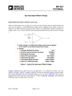
MT-037: Op Amp Input Offset Voltage - Analog Devices
www.analog.comzero volts. In practice, a small differential voltage must be applied to the inputs to force the output to zero. This is known as the input offset voltage, VOS. Input offset voltage is modeled as a voltage source, VOS, in series with the inverting input terminal of the op amp as shown in Figure 1. Rev.0, 10/08, WK Page 1 of 10 z z z z z z z
Introduction: The Nature of VCRs - Vishay Intertechnology
www.vishay.comgate control voltage, V GG, be twice as large as V GS in Fig-ure 5 for the same r DS value. Use of a floating supply be-tween the resistor junction and the FET gate will over-come this problem. The circuit is shown in Figure 7 and allows the gate control voltage to be the same value as that voltage used without a feedback circuit, while preserving
The FET Constant-Current Source/Limiter
www.vishay.comThe FET Constant-Current Source/Limiter Introduction The combination of low associated operating voltage and high output impedance makes the FET attractive as a constant-current source. An adjustable-current source (Fig-ure 1) may be built with a FET, a variable resistor, and a small battery. For optimum thermal stability, the FET should
Bootstrap Circuitry Selection for Half Bridge Configurations
www.ti.comWhen the low-side FET is turned off and the high-side is on, the HS pin of the gate driver and the switch node are pulled to the high voltage bus HV; the bootstrap capacitor discharges some of the stored voltage (accumulated during the charging sequence) to the high-side FET through the HO and HS pins of the gate driver as shown in Figure 2 ...
How to Implement a MOSFET with a Gate Driver
www.egr.msu.eduNov 13, 2014 · special type of field-effect transistor (FET) and is the key component in high frequency, high efficiency switching applications across the electronics industry. A MOSFET is a voltage controlled device. It has four terminals: a gate, a drain, a source and bulk.

NCP302155 - Integrated Driver and MOSFET
www.onsemi.comThe NCP302155 integrates a MOSFET driver, high−side MOSFET ... 27, 33 GL Low Side FET Gate Access (pin 27 and pad 33 are internally connected) 29 VCCD Driver Power Supply Input ... Input Voltage High VPWM_HI 2.65 − − V Input Mid−state Voltage VPWM_MID 1.4 − 2.1 V