Flip Chip Package Qualification of RF-IC Packages
Flip Chip Package Qualification of RF-IC Packages Mumtaz Y. Bora . Peregrine Semiconductor . San Diego, Ca. 92121 . mbora@psemi.com . Abstract. Quad Flat Pack No Leads (QFNs) are thermally enhanced plastic packages that use conventional copper leadframe with wire
Download Flip Chip Package Qualification of RF-IC Packages
Information
Domain:
Source:
Link to this page:
Documents from same domain
Failure Modes in Wire bonded and Flip Chip …
www.circuitinsight.comFailure Modes in Wire bonded and Flip Chip Packages Mumtaz Y. Bora . Peregrine Semiconductor . San Diego, Ca. 92121 . [email protected] . Abstract . The growth of portable and wireless products is driving the miniaturization of packages resulting in the development of many
Solder Joint Embrittlement Mechanisms, Solutions …
www.circuitinsight.comCase Study 1 Data . A connector pin with gold over nickel finish design was hot solder dipped with Sn63Pb37 solder alloy. The gold layer was fully dissolved.
3D IC INTEGRATION TECHNOLOGY …
www.circuitinsight.comefforts in 3D IC integration technology development by the ... semiconductor and back-end packaging assembly industry; how the industry’s growth had been planned and cultivated to arrive at the present condition. Having established such ... 3D IC INTEGRATION TECHNOLOGY DEVELOPMENT IN CHINA ...

Process Control of Ionic Contamination Achieving …
www.circuitinsight.comProcess Control of Ionic Contamination Achieving 6-Sigma Criteria in The Assembly of Electronic Circuits P. Eckold [1], M. Routley[2], L. Henneken , G. Naisbitt[2], R. Fritsch[1], U. Welzel

Electrostatic Discharge (ESD), Factory Issues, …
www.circuitinsight.comElectrostatic Discharge (ESD), Factory Issues, Measurement Methods and Product Quality – Roadmaps and Solutions for 2025 to 2030 . Dipl.-Ing. Hartmut Berndt . B.E.STAT European ESD competence centre

BEST PRACTICES REFLOW PROFILING FOR LEAD-FREE SMT …
www.circuitinsight.comThe introduction of higher lead-free process temperatures and a reduction in solder paste deposit volumes require narrower process windows to optimize the reflow profile.

INVESTIGATION AND DEVELOPMENT OF TIN-LEAD AND …
www.circuitinsight.comsolder pastes, the lead-free paste would have a higher melting temperature and be more vulnerable to oxidization with the increased temperature during pre-heat and reflow.

What is Kelvin Test? - Circuit Insight
www.circuitinsight.comWhat is Kelvin Test? Rick Meraw and Todd Kolmodin, Gardien Services USA . Manfred Ludwig, Gardien Services China . Holger Kern, Gardien Services Germany

THE DYNAMICS OF LOW STRESS EPOXY CURING
www.circuitinsight.comTHE DYNAMICS OF LOW STRESS EPOXY CURING Robert L. Hubbard, Ph.D. Lambda Technologies, Inc. Morrisville, NC, USA [email protected] Iftikhar Ahmad, Ph.D.
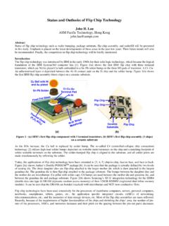
Status and Outlooks of Flip Chip Technology
www.circuitinsight.comthe organic build-up substrate, through-silicon via (TSV)-interposer, TSV-less interposer, coreless substrate, bump-on-lead (BOL), and embedded-trace-substrate (ETS) will be discussed. In order to enhance the solder joint reliability of flip chip assemblies, underfill is a must, especially for organic package substrate.
Related documents
Failure Modes in Wire bonded and Flip Chip Packages
www.circuitinsight.comFailure Modes in Wire bonded and Flip Chip Packages Mumtaz Y. Bora . Peregrine Semiconductor . San Diego, Ca. 92121 . mbora@psemi.com . Abstract . The growth of portable and wireless products is driving the miniaturization of packages resulting in the development of many

Product Specification PE4245 - psemi.com
www.psemi.comPage 1 of 8 Document No. 70-0104-07 │www.psemi.com ©2003-2009 Peregrine Semiconductor Corp. All rights reserved. The PE4245 RF Switch is designed to cover a broad ...

PE42553 - psemi.com
www.psemi.comPE42553 SPDT RF Switch Page 6 of 20 DOC-76991-2 – (11/2018) www.psemi.com Switching Frequency The PE42553 has a maximum 25 kHz switching rate in normal mode (pin 13 tied to ground).