Transcription of PE42553 - psemi.com
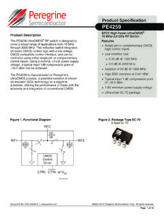
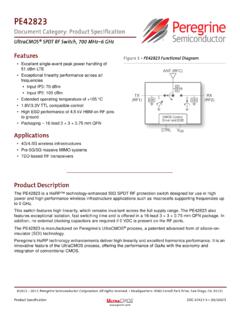
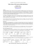
1 PE42553 . Document Category: Product Specification UltraCMOS SPDT RF Switch, 9 kHz 8 GHz Features Applications Excellent power handling: 36 dBm CW and 38 dBm Test and measurement pulsed power in 50 @ 8 GHz Signal sources High linearity: IIP3 of 66 dBm Communication testers High isolation Spectrum analyzers 45 dB @ 3 GHz Network analyzers 41 dB @ 8 GHz Automated test equipment HaRP technology enhanced General purpose TX/RX switch Fast settling time No gate and phase lag Figure 1 PE42553 Functional Diagram No drift in insertion loss and phase High ESD performance RFC. kV HBM on all pins, 4 kV HBM on RF pins to GND. 1 kV CDM on all pins RF1 RF2. Packaging 16-lead 3 3 mm QFN.
2 50 50 . CMOS Control Driver and ESD. LS CTRL VSS_EXT. Product Description The PE42553 is a HaRPTM technology-enhanced absorptive SPDT RF switch that supports a broad frequency range from 9 kHz to 8 GHz. This general purpose switch maintains excellent linearity, high RF performance and fast settling time making this device ideal for test and measurement (T&M), automated test equipment (ATE). and other high performance wireless applications. The PE42553 is a pin-compatible version of the PE42552 with improved power handling capability of 36 dBm continuous wave (CW) and 38 dBm pulsed power in 50 at 8 GHz. No blocking capacitors are required if DC. voltage is not present on the RF ports.
3 The PE42553 is manufactured on psemi 's UltraCMOS process, a patented variation of silicon-on-insulator (SOI) technology on a sapphire substrate. 2016, 2018 psemi Corporation. All rights reserved. Headquarters: 9369 Carroll Park Drive, San Diego, CA, 92121. Product Specification DOC-76991-2 (11/2018). PE42553 . SPDT RF Switch psemi 's HaRP technology enhancements deliver high linearity and excellent harmonics performance. It is an innovative feature of the UltraCMOS process, offering the performance of GaAs with the economy and integration of conventional CMOS. Optional External VSS. For proper operation, the VSS_EXT pin must be grounded or tied to the VSS voltage specified in Table 2.
4 When the VSS_EXT pin is grounded, FETs in the switch are biased with an internal negative voltage generator. For applica- tions that require the lowest possible spur performance, VSS_EXT can be applied externally to bypass the internal negative voltage generator. Absolute Maximum Ratings Exceeding absolute maximum ratings listed in Table 1 may cause permanent damage. Operation should be restricted to the limits in Table 2. Operation between operating range maximum and absolute maximum for extended periods may reduce reliability. ESD Precautions When handling this UltraCMOS device, observe the same precautions as with any other ESD-sensitive devices. Although this device contains circuitry to protect it from damage due to ESD, precautions should be taken to avoid exceeding the rating specified in Table 1.
5 Latch-up Immunity Unlike conventional CMOS devices, UltraCMOS devices are immune to latch-up. Table 1 Absolute Maximum Ratings for PE42553 . Parameter/Condition Min Max Unit Supply voltage, VDD V. Digital input voltage, CTRL V. LS input voltage V. RF input power, CW (RFC RFX)(1). 9 kHz 10 MHz Fig. 2, Fig. 3 dBm >10 MHz 8 GHz 37 dBm RF input power, pulsed (RFC RFX)(2). 9 kHz 10 MHz Fig. 2, Fig. 3 dBm >10 MHz 8 GHz Fig. 4, Fig. 5 dBm RF input power into terminated ports, CW (RFX)(1). 9 800 kHz Fig. 2, Fig. 3 dBm >800 kHz 8 GHz 28 dBm Maximum junction temperature +150 C. Storage temperature range 65 +150 C. Page 2 of 20 DOC-76991-2 (11/2018). PE42553 . SPDT RF Switch Table 1 Absolute Maximum Ratings for PE42553 .
6 Parameter/Condition Min Max Unit ESD voltage HBM(3). RF pins to GND 4000 V. All pins 2500 V. ESD voltage MM, all pins(4) 200 V. ESD voltage CDM, all pins(5) 1000 V. Notes: 1) 100% duty cycle, all bands, 50 . 2) Pulsed, 5% duty cycle of 4620 s period, 50 . 3) Human body model (MIL-STD 883 Method 3015). 4) Machine model (JEDEC JESD22-A115). 5) Charged device model (JEDEC JESD22-C101). DOC-76991-2 (11/2018) Page 3 of 20. PE42553 . SPDT RF Switch Recommended Operating Conditions Table 2 list the recommending operating condition for PE42553 . Devices should not be operated outside the recommended operating conditions listed below. Table 2 Recommended Operating Condition for PE42553 .
7 Parameter Min Typ Max Unit Normal mode (VSS_EXT = 0V)(1). Supply voltage, VDD V. Supply current, IDD 120 200 A. Bypass mode (VSS_EXT = , VDD for full spec. compliance)(2). Supply voltage, VDD V. Supply current, IDD 50 80 A. Negative supply voltage, VSS_EXT V. Negative supply current, ISS 40 16 A. Normal or Bypass mode Digital input high, CTRL V. Digital input low, CTRL V. Digital input current, ICTRL 10 A. RF input power, CW (RFC RFX)(3). 9 kHz 10 MHz Fig. 2, Fig. 3 dBm >10 MHz 8 GHz 36 dBm RF input power, pulsed (RFC RFX)(4). 9 kHz 10 MHz Fig. 2, Fig. 3 dBm >10 MHz 8 GHz Fig. 4, Fig. 5 dBm RF input power, hot switch, CW(3). 9 300 kHz Fig. 2, Fig. 3 dBm >300 kHz 8 GHz 20 dBm RF input power into terminated ports, CW (RFX)(3).
8 9 600 kHz Fig. 2, Fig. 3 dBm >600 kHz 8 GHz 26 dBm Operating temperature range 40 +25 +85 C. Notes: 1) Normal mode: connect VSS_EXT (pin 13) to GND (VSS_EXT = 0V) to enable internal negative voltage generator. 2) Bypass mode: use VSS_EXT (pin 13) to bypass and disable internal negative voltage generator. 3) 100% duty cycle, all bands, 50 . 4) Pulsed, 5% duty cycle of 4620 s period, 50 . Page 4 of 20 DOC-76991-2 (11/2018). PE42553 . SPDT RF Switch Electrical Specifications Table 3 provides the PE42553 key electrical specifications at 25 C (ZS = ZL = 50 ), unless otherwise specified. Normal mode(1) is at VDD = and VSS_EXT = 0V. Bypass mode(2) is at VDD = and VSS_EXT = Table 3 PE42553 Electrical Specifications Parameter Path Condition Min Typ Max Unit As Operating frequency 9 kHz 8 GHz shown 9 kHz 10 MHz dB.
9 Insertion loss RFC RFX 10 MHz 3 GHz dB. 3 8 GHz dB. 9 kHz 10 MHz 70 90 dB. RFX RFX 10 MHz 3 GHz 46 54 dB. 3 8 GHz 33 36 dB. Isolation 9 kHz 10 MHz 80 90 dB. RFC RFX 10 MHz 3 GHz 42 45 dB. 3 8 GHz 38 41 dB. 9 kHz 10 MHz 23 dB. Return loss (active port) RFC RFX 10 MHz 3 GHz 17 dB. 3 8 GHz 15 dB. 9 kHz 10 MHz 23 dB. Return loss RFC RFX 10 MHz 3 GHz 17 dB. (RFC port). 3 8 GHz 15 dB. 9 kHz 10 MHz 32 dB. Return loss RFX 10 MHz 3 GHz 24 dB. (terminated port). 3 8 GHz 19 dB. Input compression Fig. 4 dBm RFC RFX 10 MHz 8 GHz point(3) Fig. 5 dBm Input IP2 RFC RFX 834 MHz, 1950 MHz 120 dBm Input IP3 RFC RFX 834 MHz, 1950 MHz and 2700 MHz 66 dBm Settling time 50% CTRL to dB final value 15 20 s Switching time 50% CTRL to 90% or 10% of RF s Notes: 1) Normal mode: connect VSS_EXT (pin 29) to GND (VSS_EXT = 0V) to enable internal negative voltage generator.
10 2) Bypass mode: use VSS_EXT (pin 29) to bypass and disable internal negative voltage generator. 3) The input compression point is a linearity figure of merit. Refer to Table 2 for the RF input power (50 ). DOC-76991-2 (11/2018) Page 5 of 20. PE42553 . SPDT RF Switch Switching Frequency Control Logic The PE42553 has a maximum 25 kHz switching rate Table 5 provides the control logic truth table for the in normal mode (pin 13 tied to ground). A faster PE42553 . switching rate is available in bypass mode (pin 13 tied to VSS_EXT). The rate at which the PE42553 can be Table 5 Truth Table for PE42553 . switched is then limited to the switching time as specified in Table 3. LS CTRL RFC RF1 RFC RF2.