Transcription of Product Specification PE4245 - psemi.com
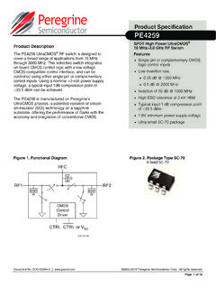
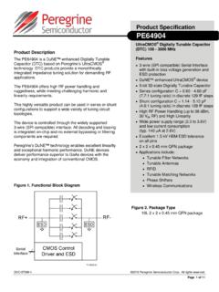
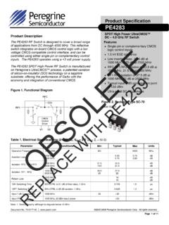
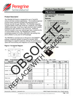
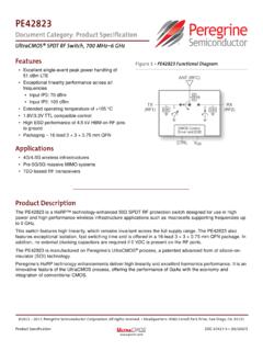
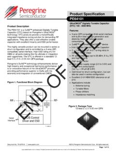
1 Product Specification PE4245 . SPDT UltraCMOS RF Switch Product Description DC - 4000 MHz The PE4245 RF Switch is designed to cover a broad range of Features applications from near DC to 4000 MHz. This switch integrates Single V Power Supply on-board CMOS control logic with a low voltage CMOS. compatible control input. Using a +3-volt nominal power Low insertion loss: dB at 1000 MHz, supply voltage, a 1 dB compression point of +27 dBm can be dB at 2000 MHz achieved. The PE4245 also exhibits excellent isolation of better than 42 dB at 1000 MHz and is offered in a small 3x3 High isolation of 42 dB at 1000 MHz, mm DFN package. 32 dB at 2000 MHz Typical 1 dB compression of +27 dBm The PE4245 is manufactured on Peregrine's UltraCMOS . process, a patented variation of silicon-on-insulator (SOI) Single-pin CMOS logic control technology on a sapphire substrate, offering the performance of GaAs with the economy and integration of conventional Available in a 6-lead DFN package CMOS.
2 Figure 1. Functional Diagram Figure 2. Package Type RFC 6-lead DFN. ESD. RF1. ESD ESD. CMOS. Control Driver CTRL. Table 1. Electrical Specifications @ +25 C, VDD = 3 V (ZS = ZL = 50 ). Parameter Conditions Minimum Typical Maximum Units Operation Frequency1 DC 4000 MHz 1000 MHz dB. Insertion Loss 2000 MHz dB. 1000 MHz 39 42 dB. Isolation RFC to RF1/RF2. 2000 MHz 30 32 dB. 1000 MHz 34 36 dB. Isolation RF1 to RF2. 2000 MHz 27 29 dB. 1000 MHz 21 23 dB. Return Loss 2000 MHz 20 22 dB. ON' Switching Time CTRL to dB final value, 2 GHz 200 ns OFF' Switching Time CTRL to 25 dB isolation, 2 GHz 90 ns Video Feedthrough2 15 mVpp Input 1 dB Compression 2000 MHz 26 27 dBm Input IP3 2000 MHz, 14 dBm 43 45 dBm Notes: 1. Device linearity will begin to degrade below 10 MHz. 2.
3 The DC transient at the output of any port of the switch when the control voltage is switched from Low to High or High to Low in a 50 test set-up, measured with 1ns risetime pulses and 500 MHz bandwidth. Document No. 70-0104-07 2003-2009 Peregrine Semiconductor Corp. All rights reserved. Page 1 of 8. Logo updated under non-rev change. Peregrine products are protected under one or more of the following Patents: PE4245 . Product Specification Figure 3. Pin Configuration Table 4. Absolute Maximum Ratings Symbol Parameter/Conditions Min Max Units RF2 1 6 RFC VDD Power supply voltage V. VDD+. Exposed Solder VI Voltage on any input V. Pad - Shorted GND 2 to Pin 2 5 CTRL. (bottom side) TST Storage temperature range -65 150 C. PIN Input power (50 ) 30 dBm RF1 3 4 VDD.
4 ESD voltage (Human Body VESD 1500 V. Model). Exceeding absolute maximum ratings may cause Table 2. Pin Descriptions permanent damage. Operation should be restricted to the limits in the Operating Ranges Pin Pin table. Operation between operating range Description No. Name maximum and absolute maximum for extended 1 RF2 RF2 port (Note 1) periods may reduce reliability. Ground Connection. Traces should be physically short and connected to the ground plane. This pin is connected to 2 GND. the exposed solder pad that also must be soldered to the ground plane for best Table 5. Control Logic Truth Table performance. Control Voltage Signal Path 3 RF1 RF1 port (Note 1). CTRL = CMOS High RFC to RF1. 4 VDD Nominal 3 V supply connection. CTRL = CMOS Low RFC to RF2. CMOS logic level: 5 CTRL High = RFC to RF1 signal path Low = RFC to RF2 signal path Electrostatic Discharge (ESD) Precautions 6 RFC Common RF port for switch (Note 1) When handling this UltraCMOS device, observe the same precautions that you would use with Notes: 1.
5 All RF pins must be DC blocked with an external series capacitor or held at 0 VDC. other ESD-sensitive devices. Although this device contains circuitry to protect it from damage due to ESD, precautions should be taken to avoid Table 3. Operating Ranges exceeding the rating specified in Table 4. Parameter Min Typ Max Units Latch-Up Avoidance VDD Power Supply Voltage V. Unlike conventional CMOS devices, UltraCMOS . IDD Power Supply Current devices are immune to latch-up. 250 500 nA. VDD = 3V, VCTRL = 3V. TOP Operating temperature -40 85 C. range Control Voltage High V. VDD. Control Voltage Low V. VDD. Moisture Sensitivity Level The Moisture Sensitivity Level rating for the PE4245 in the 6-lead 3x3 DFN package is MSL1. 2003-2009 Peregrine Semiconductor Corp. All rights reserved.
6 Document No. 70-0104-07 UltraCMOS RFIC Solutions Page 2 of 8. Logo updated under non-rev change. Peregrine products are protected under one or more of the following Patents: PE4245 . Product Specification Typical Performance Data @ 25 C (Unless Otherwise Noted). Figure 4. Insertion Loss - RFC to RF1 Figure 5. Input 1dB Compression Point and IIP3. T = -40 C to 85 C. 0 60 60. -40 C. 50 50. 1dB Compression Point (dBm). Insertion Loss (dB). IIP3 (dBm). 40 40. 85 C 25 C. 30 30. 0 800 1600 2400 3200 4000 20 20. 0 800 1600 2400 3200 4000. Frequency (MHz). Frequency (MHz). Figure 6. Insertion Loss - RFC to RF2 Figure 7. Isolation - RFC to RF1. T = -40 C to 85 C. 0 0. -40 C. -20. Insertion Loss (dB). -40. Isolation (dB). 85 C 25 C. -60. -80. -100. 0 800 1600 2400 3200 4000 0 800 1600 2400 3200 4000.
7 Frequency (MHz) Frequency (MHz). Document No. 70-0104-07 2003-2009 Peregrine Semiconductor Corp. All rights reserved. Page 3 of 8. Logo updated under non-rev change. Peregrine products are protected under one or more of the following Patents: PE4245 . Product Specification Typical Performance Data @ 25 C. Figure 8. Isolation RFC to RF2 Figure 9. Isolation RF1 to RF2, RF2 to RF1. 0 0. -20. -25. -40. Isolation (dB). Isolation (dB). -50. -60. -75. -80. -100 -100. 0 800 1600 2400 3200 4000 0 800 1600 2400 3200 4000. Frequency (MHz) Frequency (MHz). Figure 10. Return Loss RFC to RF1, RF2 Figure 11. Return Loss RF1, RF2. 0 0. -10 -10. Return Loss (dB). Return Loss (dB). RF1. -20 -20. RF1. RF2. -30 -30. RF2. -40 -40. 0 800 1600 2400 3200 4000 0 800 1600 2400 3200 4000.
8 Frequency (MHz) Frequency (MHz). 2003-2009 Peregrine Semiconductor Corp. All rights reserved. Document No. 70-0104-07 UltraCMOS RFIC Solutions Page 4 of 8. Logo updated under non-rev change. Peregrine products are protected under one or more of the following Patents: PE4245 . Product Specification Evaluation Kit Figure 12. Evaluation Board Layouts Peregrine Specification 101/0085. The SPDT Switch Evaluation Kit board was designed to ease customer evaluation of the PE4245 SPDT switch. The RF common port is connected through a 50 transmission line to the top left SMA connector, J1. Port 1 and Port 2 are connected through 50 transmission lines to the top two SMA connectors on the right side of the board, J2 and J3. A through transmission line connects SMA connectors J4 and J5.
9 This transmission line can be used to estimate the loss of the PCB over the environmental conditions being evaluated. The board is constructed of a two metal layer FR4. material with a total thickness of . The bottom layer provides ground for the RF. transmission lines. The transmission lines were designed using a coplanar waveguide with ground plane model using a trace width of , trace gaps of , dielectric thickness of , metal thickness of and r of J6 provides a means for controlling DC and digital inputs to the device. Starting from the lower left pin, the second pin to the right (J6-3) is connected to the device CTRL input. The fourth pin to the right (J6-7) is connected to the device VDD input. Figure 13. Evaluation Board Schematic Peregrine Specification 102/0110.
10 Document No. 70-0104-07 2003-2009 Peregrine Semiconductor Corp. All rights reserved. Page 5 of 8. Logo updated under non-rev change. Peregrine products are protected under one or more of the following Patents: PE4245 . Product Specification Figure 14. Package Drawing 6-lead DFN. (3x3mm). 06L SLP. NOTE: The exposed solder pad (on the bottom of the package) is electrically connected to pin 2 (fused.). Figure 15. Marking Specifications 4245. YYWW. ZZZZZ. YYWW = Date Code (last two digits of year and work week). ZZZZZ = Last five digits of Lot Number 2003-2009 Peregrine Semiconductor Corp. All rights reserved. Document No. 70-0104-07 UltraCMOS RFIC Solutions Page 6 of 8. Logo updated under non-rev change. Peregrine products are protected under one or more of the following Patents: PE4245 .