
Flip-Flops and Sequential Circuit Design
February 13, 2012 ECE 152A - Digital Design Principles 2 Reading Assignment Brown and Vranesic 7Flip-Flops, Registers, Counters and a Simple Processor 7.5 T Flip-Flop 7.5.1 Configurable Flip-Flops 7.6 JK Flip-Flop 7.7 Summary of Terminology 7.8 Registers 7.8.1 Shift Register 7.8.2 Parallel-Access Shift Register
Download Flip-Flops and Sequential Circuit Design

Information
Domain:
Source:
Link to this page:
Documents from same domain
Transistor Technologies for High Efficiency and Linearity
web.ece.ucsb.eduDifferential Topology • Double the available voltage swing • Even-order harmonic suppression • Double the frequency of current injection into substrate –Reduce the potential for LO-pulling • The tail current source is removed from the standard differential pair (this is a “quasi-differential” structure) –DC current set by the biasing of input devices

Phase Locked Loop Circuits
web.ece.ucsb.eduClock generation: B. Razavi, Design of Analog CMOS Integrated Circuits, Chap. 15, McGraw-Hill, 2001. 1. Definition. A PLL is a feedback system that includes a VCO, phase detector, and low pass filter within its loop. Its purpose is to force the VCO to replicate and track the frequency and phase at the input when in lock.

ADS Tutorial Stability and Gain Circles ECE145A/218A
web.ece.ucsb.eduequations. The syntax is: gp_circle(S, gain, # points on circle) where S is the S-parameter matrix. Let’s illustrate. In the example below, a table is used to display frequency, maximum stable gain (MSG), the stability factor, k, and the magnitude of delta. The gain circles are at MSG (MaxGain1 in this case), and 1 and 2 dB below MSG.
Audio Amplifier Circuit - UC Santa Barbara
web.ece.ucsb.eduWeek #1: Audio amplifier Week #2: Microphone circuit The audio amplifier project is more difficult and time-consuming than the microphone pre-amp, so part of week #2 may be used to finish the audio amp. All breadboarding and testing can and should be done in lab. Soldering and hardwiring can and should be done outside lab.

Harmonic Balance Simulation on ADS
web.ece.ucsb.eduHarmonic Balance Simulation on ADS General Description of Harmonic Balance in Agilent ADS 1 Harmonic balance is a frequency-domain analysis technique for simulating nonlinear circuits and systems. It is well-suited for simulating analog RF and microwave circuits, ... function is driven to a given small value), then the resulting voltage ...
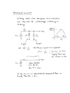
Quality factor, Q
web.ece.ucsb.eduWhen a resonant circuit is connected to the outside world, its total losses (let’s call them RP or GP) are combined with the source and load resistances, RS and RL. For example, Here is a parallel resonant circuit (C,L and RP)connected to the outside. The total Q of this circuit is called the loaded Q or QL and is given by

Latches, the D Flip-Flop & Counter Design
web.ece.ucsb.eduFebruary 6, 2012 ECE 152A - Digital Design Principles 2 Reading Assignment Brown and Vranesic 7Flip-Flops, Registers, Counters and a Simple Processor 7.1 Basic Latch 7.2 Gated SR Latch 7.2.1 Gated SR Latch with NAND Gates 7.3 Gated D …

BASICS OF THE SPECTRUM ANALYZER - UC Santa Barbara
web.ece.ucsb.eduFourier ⋅ π → − + + Now instead of a bank of narrow filters, we shall have one narrow filter centered at a fixed frequency, say fI, and we shall scan the signal spectrum across this filter by multiplying x(t) by a sinusoid of varying frequency f0. See Figure 1. …

Mealy and Moore Machines
web.ece.ucsb.eduFebruary 22, 2012 ECE 152A - Digital Design Principles 5 Finite State Machines Two types (or models) of sequential circuits (or finite state machines) Mealy machine Output is function of present state and present input Moore machine Output is function of present state only Analysis first, then proceed to the design of
Number Representation and Computer Arithmetic
web.ece.ucsb.eduOne way to encode decimal digits using binary signals is to encode each of the digits 0-9 by means of its 4-bit binary representation. The resulting binary-coded decimal (BCD) representation is shown below:
Related documents

7. Latches and Flip-Flops
www.cs.ucr.eduChapter 7 – Latches and Flip-Flops Page 3 of 18 a 0. When both inputs are de-asserted, the SR latch maintains its previous state. Previous to t1, Q has the value 1, so at t1, Q remains at a 1. Similarly, previous to t3, Q has the value 0, so at t3, Q remains at a 0. If both S' and R' are asserted, then both Q and Q' are equal to 1 as shown at time t4.If one of the input signals is
Metastability - University of Southern California
www-classes.usc.edutypically described by four measurements of flip-flop performance — MTBF, T, To and tr. MTBF is the “mean-time-between-failure” of a flip-flop. where tr is metastability resolution time, maximum time the output can remain metastable without causing synchronizer failure. …

Circuits with Flip-Flop = Sequential Circuit Circuit ...
www.cse.psu.edu1 flip-flop => 2 states 2 flip-flops => 4 states 3 flip3 flip-flops => 8 statesflops => 8 states 4 flip-flops => 16 states. Sequential circuit components: Circuit, State Diagram, State Table Sequential circuit components Flip-flop(s) Clock Logic gates Input Output. State diagram:

Dual D-type flip-flop
assets.nexperia.comDual D-type flip-flop Rev. 10 — 23 November 2021 Product data sheet 1. General description The HEF4013B is a dual D-type flip-flop with set and reset; positive-edge trigger. Inputs include clamp diodes. This enables the use of current limiting resistors to interface inputs to voltages in excess of VDD. 2. Features and benefits
Latches, the D Flip-Flop & Counter Design
web.ece.ucsb.eduFebruary 6, 2012 ECE 152A - Digital Design Principles 3 Reading Assignment Brown and Vranesic (cont) 7Flip-Flops, Registers, Counters and a Simple Processor (cont) 7.4 Master-Slave and Edge-Triggered D Flip-Flops 7.4.1 Master-Slave D Flip-Flop 7.4.2 Edge-Triggered D Flip-Flop 7.4.3 D Flip-Flop with Clear and Preset 7.4.4 Flip-Flop Timing Parameters (2nd edition)

Introduction to Digital Electronics
www.agner.org3 1. Number systems 1.1. Decimal, binary, and hexadecimal numbers We all know the decimal number system. For example, 2019 means 2*1000 + 0*100 + 1*10 + 9*1.
7. Latches and Flip-Flops
www.cs.ucr.eduChapter 7 – Latches and Flip-Flops Page 3 of 18 a 0. When both inputs are de-asserted, the SR latch maintains its previous state. Previous to t1, Q has the value 1, so at t1, Q remains at a 1. Similarly, previous to t3, Q has the value 0, so at t3, Q remains at a 0. If both S' and R' are asserted, then both Q and Q' are equal to 1 as shown at time t4.If one of the input signals is

MC74HC74A - Dual D Flip-Flop with Set and Reset
www.onsemi.comDual D Flip-Flop with Set and Reset High−Performance Silicon−Gate CMOS The MC74HC74A is identical in pinout to the LS74. The device inputs are compatible with standard CMOS outputs; with pullup resistors, they are compatible with LSTTL outputs. This device consists of two D flip−flops with individual Set, Reset, and Clock inputs.

Modeling Latches and Flip-flops - Xilinx
www.xilinx.comflip-flop can be viewed as a memory cell or a delay line. The active edge in a flip-flop could be rising or falling. The following figure shows rising (also called positive) edge triggered D flip-flop and falling (negative edge) triggered D flip-flop. The positive edge triggered D flip-flop can be modeled using behavioral modeling as shown below.

Modeling Latches and Flip-flops - Xilinx
www.xilinx.comflip-flop can be viewed as a memory cell or a delay line. The active edge in a flip-flop could be rising or falling. The following figure shows rising (also called positive) edge triggered D flip-flop and falling (negative edge) triggered D flip-flop. The positive edge triggered D flip-flop can be modeled using behavioral modeling as shown ...