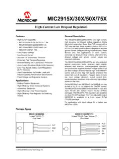
High-Current Low Dropout Regulators
Aug 15, 2018 · 5: Dropout voltage is defined as the input-to-output differential when the output voltage drops to 99% of its normal value with VOUT + 1V applied to VIN. 6: Ground pin current is the regulator quiescent current. The total current drawn from the source is the sum of the load current plus the ground pin current. 7: VIN = VOUT (nominal) + 1V.
Download High-Current Low Dropout Regulators

Information
Domain:
Source:
Link to this page:
Documents from same domain

Power Factor Correction in Power Conversion …
ww1.microchip.com© 2007 Microchip Technology Inc. DS01106A-page 2 AN1106 FIGURE 1: CURRENT WAVEFORMS WITH AND WITHOUT PFC These waveforms illustrate that …

2.7V to 5.5V Single Supply CMOS Op Amp
ww1.microchip.comMCP601/1R/2/3/4 DS21314G-page 2 © 2007 Microchip Technology Inc. 1.0 ELECTRICAL CHARACTERISTICS Absolute Maximum Ratings † VDD –VSS.....7.0V

Data Encryption Routines for PIC24 and dsPIC Device
ww1.microchip.com© 2006 Microchip Technology Inc. DS01044A-page 1 AN1044 INTRODUCTION Currently, there are three data encryption standards approved …

Using SAM-BA for Linux on SAMA5D3 Xplained
ww1.microchip.comAN-8995 – Using SAM-BA for Linux on SAMA5D3 Xplained: 42328A−06/2014 Page 5 of 19 2. Setup With Ubuntu distributions, a user has to be member of the dialout group to access serial devices like

MCP6021/1R/2/3/4 - Rail-to-Rail Input/Output, 10 …
ww1.microchip.com2001-2017 Microchip Technology Inc. DS20001685E-page 1 MCP6021/1R/2/3/4 Features • Rail-to-Rail Input/Output • Wide Bandwidth: 10 MHz (typical)

Low Quiescent Current LDO - Microchip Technology
ww1.microchip.com2005-2016 Microchip Technology Inc. DS20001826D-page 1 MCP1700 Features: • 1.6 µA Typical Quiescent Current • Input Operating Voltage Range: 2.3V to 6.0V

MCP1703 250 mA, 16V, Low Quiescent Current
ww1.microchip.com2010 Microchip Technology Inc. DS22049E-page 1 MCP1703 Features: • 2.0 µA Typical Quiescent Current • Input Operating Voltage Range: 2.7V to16.0V

MTCH6102 Low-Power Projected Capacitive Touch …
ww1.microchip.com2014 Microchip Technology Inc. DS40001750A-page 1 Description: Microchip’s MTCH6102 is a turnkey projected capacitive touch controller that simplifies adding

PIC32 GUI Development Board with Projected …
ww1.microchip.comPIC32 GUI Development Board with Projected Capacitance (PCAP) Touch Information Sheet Microchip Technology Inc.

RN4020 Bluetooth Low Energy Module User’s Guide
ww1.microchip.comRN4020 BLUETOOTH LOW ENERGY MODULE USER’S GUIDE 2014 Microchip Technology Inc. DS70005191B-page 7 Preface INTRODUCTION This chapter contains general information that will be useful to know before using the
Related documents
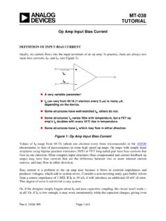
MT-038: Op Amp Input Bias Current - Analog Devices
www.analog.comOp Amp Input Bias Current . DEFINITION OF INPUT BIAS CURRENT . Ideally, no current flows into the input terminals of an op amp. In practice, there are always two input bias currents, IB+ and IB-(see Figure 1). Rev.0, 10/08, WK Page 1 of 5 A very variable parameter! I B can vary from 60 fA (1 electron every 3 μs) to many μA,

LF353-NWide Bandwidth Dual JFET Input Operational Amplifier
www.ti.comThese devices are low cost, high speed, dual JFET 2• Internally Trimmed Offset Voltage: 10 mV input operational amplifiers with an internally trimmed • Low Input Bias Current: 50pA input offset voltage (BI-FET II technology). They • Low Input Noise Voltage: 25 nV/√Hz require low supply current yet maintain a large gain
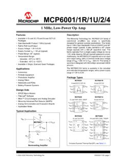
MCP6001/1R/1U/2/4 - 1 MHz, Low-Power Op Amp
ww1.microchip.comMay 14, 2019 · family operates from a single-supply voltage as low as 1.8V, while drawing 100 µA (typical) quiescent current. Additionally, the MCP6001/2/4 supports rail-to-rail input and output swing, with a Common-mode input voltage range of V DD + 300 mV to V SS – 300 mV. This family of op amps is designed with Microchip’s advanced CMOS process.

OPA657 1.6-GHz, Low-Noise, FET-Input Operational Amplifier ...
www.ti.com• Low-Input Bias Current: 2 pA a single OPA657 gain stage with exceptional • Low-Input Voltage Noise: 4.8 nV/√Hz bandwidth and accuracy. Having a high 1.6-GHz gain • High-Output Current: 70 mA bandwidth product gives greater than 10-MHz signal • Fast Overdrive Recovery bandwidths up to gains of 160 V/V (44 dB). The very low input bias ...
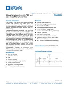
MAX9814 - Microphone Amplifier with AGC and Low-Noise ...
datasheets.maximintegrated.comThe MAX9814 is a low-cost, high-quality microphone amplifier with automatic gain control (AGC) and low-noise microphone bias. The device features a low-noise preamplifier, variable gain amplifier (VGA), output amplifier, microphone-bias-voltage generator, and AGC control circuitry. The low-noise preamplifier has a fixed 12dB gain, while
Lecture 20 - MIT
web.mit.edu• A current buffer takes the input current which may have a relatively small Norton resistance and replicates the current at the output port, which has a high output resistance • Input signal is applied to the source • Output is taken from the drain • To first order, current gain ≈1 –is ≈-iout.(Current Buffer) • Input resistance ...
Bias Circuits for RF Amplifiers - QSL.net
www.qsl.net• For good gain characteristics, it is necessary to bias the transistor at a collector current that results in maximum or near-maximum f t. • On the other hand, for best noise characteristics, a low current is generally most desirable. Finally, one must consider the maximum signal level expected at the input of the transistor.
Femtoampere Input Bias Current Electrometer Amplifier Data ...
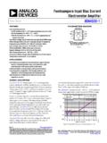
www.analog.comLow input bias current ±20 fA maximum at T A = 25°C (guaranteed at production test) ±20 fA maximum at −40°C < T. A < +85°C . ±250 fA maximum at −40°C < T. A < +125°C (guaranteed at production test) Low offset voltage: 50 µV maximum over specified CMRR range . Offset voltage drift: ±0.13 µV/ °C typical, ±0.5 µV/°C maximum