
How to Build a Printed Circuit Board
Resist Strip The developed dry film resist is now removed from the panel. The tin plating is not affected. Any holes that were covered with resist are now open and will be non-plated. This is the first step in the common phrase “strip-etch-strip”or …
Download How to Build a Printed Circuit Board
Information
Domain:
Source:
Link to this page:
Documents from same domain
How to Build a Printed Circuit Board
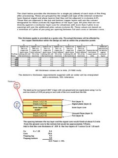
www.4pcb.comAdvanced Circuits Inc 2004 3 Single & Double Sided Circuit Boards A single sided board is made from rigid laminate consisting of a woven glass epoxy base

PCB Artist Tutorial - Advanced Circuits
www.4pcb.comChapter 1 – Getting Started 5 Chapter 1. Getting Started Introduction to PCB Artist Welcome to the PCB Artist electronic design system. The system is …
Prepreg thickness chart - Advanced Circuits
www.4pcb.comPrepreg Signal Ground Foil Signal Ground Foil Signal Ground Foil 106 1.8 1.9 2.0 1.7 1.8 1.9 1.5 1.6 1.7 1080 2.4 2.6 2.8 2.3 2.5 2.8 2.1 2.3 …

Via In Pad - Conductive Fill or Non-Conductive Fill
www.4pcb.comVia In Pad - Conductive Fill or Non-Conductive Fill? “Which is the Best Choice for My Design?” One of the most commonly asked questions when deciding how to …

Highly Reliable Via-In-Pad Design - Advanced Circuits
www.4pcb.comTECH TALK FOR TECHIES "Highly Reliable Via-In-Pad Design" Via-In-Pad (VIP) is rapidly becoming more commonly used in modern printed circuit design due to
Via In Pad - Conductive Fill or Non-Conductive Fill
www.4pcb.comof the padstack structures move either with or against the adjacent board laminate material, which can lead to stress fractures and possible electrical opens in the very worst cases. This consideration naturally favors the non-conductive epoxies as their CTE is a better match with the laminate therefore making a more reliable overall structure.
Prepreg Thickness Chart - USA PCB Manufacturer & Assembly
www.4pcb.comPrepreg Signal Ground Foil Signal Ground Foil Signal Ground Foil 106 1.8 1.9 2.0 1.7 1.8 1.9 1.5 1.6 1.7 1080 2.4 2.6 2.8 2.3 2.5 2.8 2.1 2.3 2.6 2116 4.0 4.2 4.9 3.9 ...
Related documents

An Overview of Forging Processes with Their Defects - IJSRP
www.ijsrp.orgdefects that are lightly to come if a proper care is not taken in forging process design. Defects can be defined as the ... to resist abrasion wear due to scales present on work piece. Selection of proper die material depends on: Die size, Composition and properties of …

Yield and Yield Management - Smithsonian Institution
smithsonianchips.si.eduvolume can be attributed to random defects. The other main contributors to yield loss include design margin and process variation, followed by photolithography errors, and material (wafer) defects (Figure 3-2). The dramatic decline in the contribution of people to particulate problems in the fab can be attributed to better education and train-

WARNING: This product contains chemicals known to the ...
www.crimsontrace.comLaser sights require minimal attention and are designed to resist most common firearm chemicals and lubricants, however, excessive exposure to these chemicals can be detrimental. ... warrants that this product will be free from defects in materials and workmanship for a period of three years from the original retail purchase. CTC will repair or ...

Spin-coating of Photoresists - MicroChemicals
microchemicals.comthe resist fi lm becomes suffi ciently stable to suppress its elapsing during the handling of the wafers after coating. Advantages The spin-coating of the resist typically takes only 10 - 20 sec- ... Inhomogeneous Resist Film Thickness and Resist Defects Textured Substrates.

Photolithography Overview for MEMS
nanoscale.unl.eduThe amount of resist applied and the amount of time that the wafer spins d. The spin speed of the wafer after deposition of resist and the viscosity of the resist 9. During the coating of photoresist, the thickness of the photoresist _____ with an increase in spin speed. ... Defects (particles, scratches, etc.) 17. The final test on a micro ...

Defect in crystals - Weizmann Institute of Science
www.weizmann.ac.ilPoints defects Self-interstitial –A self-interstitial is an atom from the crystal that is crowded into an interstitial site, a small void space that under ordinary circumstances is not occupied. the formation of this defect is not highly probable, and it exists in

Temperature Dependence of Semiconductor Conductivity
www.iiserkol.ac.inImpurity scattering is caused by crystal defects such as ionized impurities. At lower temperatures, carriers move more slowly, so there is more time for them to interact with charged impurities. As a result, as the temperature decreases, impurity scattering increases, and the mobility decreases.
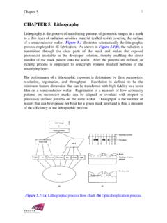
CHAPTER 5: Lithography - City University of Hong Kong
www.cityu.edu.hkcause defects in the devices. As illustrated in Figure 5.2, airborne particles adhering to the surface of a photomask behave as opaque patterns that can be ... patterns onto a resist-coated wafer many centimeters away from the mask. The small image area is scanned or stepped over the wafer to cover the entire surface.

Lecture 25: Lithography
nptel.ac.inexcess resist is removed, and there is a uniform lm over the entire surface. The right amount of resist should be added, so that coverage is uniform but not excessive, as shown in gure 10. The nal resist thickness depends on the amount of resist, spin speed, viscosity, surface tension, and drying char-acteristics (solvent dependent).