MOSFET Device Physics and Operation
the mobile charge in the channel by capacitive coupling (field effect). Examples of FETs based on these principles are metal-oxide-semiconductor FET (MOSFET), junction FET (JFET), metal-semiconductor FET (MESFET), and heterostructure FET (HFETs). In all cases, the stationary gate-channel impedance is very large at normal operating conditions.
Download MOSFET Device Physics and Operation

Information
Domain:
Source:
Link to this page:
Documents from same domain
MOSFET Device Physics and Operation
homepages.rpi.edu1 MOSFET Device Physics and Operation 1.1 INTRODUCTION A field effect transistor (FET) operates as a conducting semiconductor channel with two ohmic contacts – the source and the drain – where the number of charge carriers in the
FTIR and DSC of polymer films used for packaging: …
homepages.rpi.edu2 Samples: The pictures of the polymeric material samples that we used in this experiment are shown in figure 1. These samples are used in …
Advances in Radiation Detection and Measurement
homepages.rpi.edu506 Transactions of the American Nuclear Society, Vol. 113, Washington, D.C., November 8–12, 2015 Advances in Radiation Detection and Measurement

Industrial Growth and Competition
homepages.rpi.eduIndustrial Growth and Competition K. Simons, 2003 3 5. Sources of Invention: Big Firms & Streamlined Structure, Improvement & Efficiency.....48

Introduction to Stochastic Processes MATH 6790 | Fall 2008
homepages.rpi.eduKarlin and Taylor, A First Course in Stochastic Processes, Second Edition: A rather advanced textbook with many interesting examples and a rather thorough theoretical development of …

Stock Rocker Vs Roller Rocker
homepages.rpi.eduand the inside of the rocker was cut away using the shell command. This created a relatively thin ... negligible in comparison to the spring load. Calculation 1 shows the calculations for the force on ... Stock Rocker vs Roller Rocker .

Useful Stata Commands (for Stata versions 13, 14, & 15 ...
homepages.rpi.eduKenneth L. Simons, 19-Apr-18 1 Useful Stata Commands (for Stata versions 13, 14, & 15) Kenneth L. Simons – This document is updated continually. For the latest version, open it …
Useful Stata Commands 2019
homepages.rpi.eduThis document briefly summarizes Stata commands useful in ECON-4570 Econometrics and ECON-6570 Advanced Econometrics. This presumes a basic working knowledge of how to open Stata, use the menus, use the data editor, and use the do-file editor. We will cover these topics in early Stata sessions in class. If you miss the

Prof. Suvranu De Linear shape functions in 1D Quadratic ...
homepages.rpi.edu• Linear shape functions in 1D • Quadratic and higher order shape functions • Approximation of strains and stresses in an element Axially loaded elastic bar x y x=0 x=L A(x) = cross section at x b(x) = body force distribution (force per unit length) E(x) = Young’s modulus x F Potential energy of the axially loaded bar corresponding to the
Electron mean free path in elemental metals
homepages.rpi.eduand the projector-augmented wave method.35 Computational convergence with respect to the energy cut-off for the plane wave expansion, the k-point grid, and the unit cell size and shape is tested and adjusted such that all values reported in this letter have a computational uncertainty<1%. In addition
Related documents
ADTL082/ADTL084 Low Cost JFET Input Operational …
www.analog.comThe ADTL082 and ADTL084 are JFET input amplifiers that provide industry-leading performance over TL08x devices. The ADTL082A and ADTL084A are improved versions of TL08x A, I, and Q grades. The ADTL082J and ADTL084J are industry alternatives to the TL08x standard and C grades. The ADTL08x family offers lower noise, offset voltage, offset
5.11 THE JUNCTION FIELD-EFFECT TRANSISTOR (JFET)
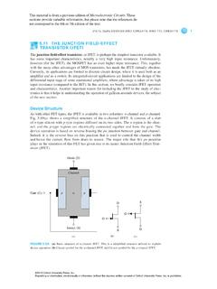
global.oup.comThe p-Channel JFET The current–voltage characteristics of the p-channel JFET are described by the same equa-tions as the n-channel JFET. Note, however, that for the p-channel JFET, VP is positive,, vDS is negative, λ and VA are negative, and …
Low-noise JFET quad operational amplifier
www.st.comJul 07, 2008 · JFET input single operational amplifiers. Each of these JFET input operational amplifiers incorporates well matched, high-voltage JFET and bipolar transistors in a monolithic integrated circuit. The devices feature high slew rates, low input bias and offset currents, and low offset voltage temperature coefficient. Inverting Input 2
Field Effect Transistors in Theory and Practice ...
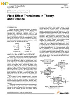
www.nxp.comreversed and the channel begins to deplete of carriers as seen in Figure 8. As with the JFET, drain-current flow depletes the channel area nearest the drain first. The structure of Figure 7, therefore, is both a depletion-mode and an enhancement-mode device. MODES OF OPERATION There are two basic modes of operation of FET’s — depletion and ...
Power MOSFET Basics: Understanding MOSFET Characteristics ...
www.vishay.combackside. The channel is formed under the polysilicon gate layer along the planar surface. However, the planar structure has an effective finite level of cell density because the JFET pinch-off effect 3 leads to an increased device on-resistance, compared with the Trench structure, at very high cell densities.

Field Effect Transistors - Learn About Electronics
learnabout-electronics.orgJFET Circuit Symbols P channel JFETs are also available and the principle of operation is the same as the N channel type described here, but polarities of the voltages are of course reversed, and the charge carriers are holes. Notice in the JFET circuit symbols shown in Fig.
Chapter 9: FET Amplifiers And Switching Circuits
staff-old.najah.eduThe ac analysis is the same as for the JFET amplifier. 9-1: The Common Source Amplifier E-MOSFET Amplifier Operation: A voltage divider common-source amplifier for n-channel E-MOSFET is shown. The gate is biased with a positive voltage such that VGS > VGS(th) Dc analysis Ac analysis where Voltage gain is same as for JFET m d gs ds in out v g R ...
J111, J112 - JFET Chopper Transistors
www.onsemi.comJFET Chopper Transistors N−Channel — Depletion Features • Pb−Free Packages are Available* MAXIMUM RATINGS Rating Symbol Value Unit Drain−Gate Voltage VDG −35 Vdc Gate−Source Voltage VGS −35 Vdc Gate Current IG 50 mAdc Total Device Dissipation @ TA = 25°C Derate above = 25°C PD 350 2.8 mW mW/°C Lead Temperature TL 300 °C ...

ON Semiconductor Is Now
www.onsemi.comN−Channel − Depletion N−Channel Junction Field Effect Transistors, depletion mode (Type A) designed for audio and switching applications. Features • N−Channel for Higher Gain • Drain and Source Interchangeable • High AC Input Impedance • High DC Input Resistance • Low Transfer and Input Capacitance