Example: bankruptcy
ON Semiconductor Is Now
N−Channel − Depletion N−Channel Junction Field Effect Transistors, depletion mode (Type A) designed for audio and switching applications. Features • N−Channel for Higher Gain • Drain and Source Interchangeable • High AC Input Impedance • High DC Input Resistance • Low Transfer and Input Capacitance
Tags:
Information
Domain:
Source:
Link to this page:
Documents from same domain

BSS138 N-Channel Logic Level Enhancement Mode …
www.onsemi.com2005 Semiconductor Components Industries, LLC. September-2017, Rev. 3 Publication Order Number: BSS138/D BSS138 N-Channel Logic Level Enhancement Mode Field Effect Transistor

BCP56T1 - NPN Silicon Epitaxial Transistor
www.onsemi.com© Semiconductor Components Industries, LLC, 2016 March, 2018 − Rev. 14 1 Publication Order Number: BCP56T1/D BCP56 Series NPN Silicon Epitaxial Transistor These NPN Silicon Epitaxial transistors are designed for use in

AN1040/D Mounting Considerations For Power …
www.onsemi.comSemiconductor Components Industries, LLC, 2001 May, 2001 – Rev. 3 1 Publication Order Number: AN1040/D AN1040/D Mounting Considerations For Power Semiconductors

Corporate Fact Sheet - ON Semiconductor
www.onsemi.comCompany Profile ON Semiconductor (Nasdaq: ON) is driving energy efficient innovations, empowering customers to reduce global energy use. The company is a leading supplier of semiconductor-based

AND8231 - Circuit Configuration Options for TVS …
www.onsemi.comAND8231/D www.onsemi.com 2 Avalanche TVS Diodes Avalanche diodes are a good TVS device for applications that require power line surge immunity and ESD protection.

BCP53 Series PNP Silicon Epitaxial Transistors
www.onsemi.comBCP53 Series www.onsemi.com 3 TYPICAL CHARACTERISTICS Figure 1. Collector Emitter Saturation Voltage vs. Collector Current Figure 2. DC Current Gain vs. Collector

AND8299 - EMC Tests and PCB Guidelines for …
www.onsemi.comAND8299 - EMC Tests and PCB Guidelines for Automotive Linear Regulators

TND310 ON Semiconductor Device Nomenclature
www.onsemi.comThis document contains the device nomenclature breakdown (also referred to as the part number decoder, product naming convention, or part naming convention) for …

LP2950 - 100 mA, Low Power Low Dropout Voltage …
www.onsemi.comLP2950, LP2951, NCV2951 www.onsemi.com Dropout Voltage V 0 in LP2950/LP2951 BIAS CURRENT (mA) I = 25°C V

2018 PHILIPPINES BENEFITS SUMMARY - ON …
www.onsemi.com2018 PHILIPPINES BENEFITS SUMMARY Employees are eligible for most benefits program on the first day of employment. Holidays: Ten (10) paid national regular holidays and Eight (8) national special holidays per year as provided
Related documents
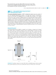
5.11 THE JUNCTION FIELD-EFFECT TRANSISTOR (JFET)
global.oup.comThe p-Channel JFET The current–voltage characteristics of the p-channel JFET are described by the same equa-tions as the n-channel JFET. Note, however, that for the p-channel JFET, VP is positive,, vDS is negative, λ and VA are negative, and …

Field Effect Transistors - Learn About Electronics
learnabout-electronics.orgJFET Circuit Symbols P channel JFETs are also available and the principle of operation is the same as the N channel type described here, but polarities of the voltages are of course reversed, and the charge carriers are holes. Notice in the JFET circuit symbols shown in Fig.
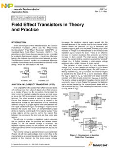
Field Effect Transistors in Theory and Practice ...
www.nxp.comreversed and the channel begins to deplete of carriers as seen in Figure 8. As with the JFET, drain-current flow depletes the channel area nearest the drain first. The structure of Figure 7, therefore, is both a depletion-mode and an enhancement-mode device. MODES OF OPERATION There are two basic modes of operation of FET’s — depletion and ...
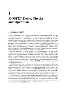
MOSFET Device Physics and Operation
homepages.rpi.eduthe mobile charge in the channel by capacitive coupling (field effect). Examples of FETs based on these principles are metal-oxide-semiconductor FET (MOSFET), junction FET (JFET), metal-semiconductor FET (MESFET), and heterostructure FET (HFETs). In all cases, the stationary gate-channel impedance is very large at normal operating conditions.
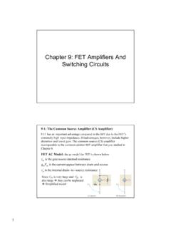
Chapter 9: FET Amplifiers And Switching Circuits
staff-old.najah.eduThe ac analysis is the same as for the JFET amplifier. 9-1: The Common Source Amplifier E-MOSFET Amplifier Operation: A voltage divider common-source amplifier for n-channel E-MOSFET is shown. The gate is biased with a positive voltage such that VGS > VGS(th) Dc analysis Ac analysis where Voltage gain is same as for JFET m d gs ds in out v g R ...
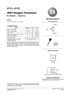
J111, J112 - JFET Chopper Transistors
www.onsemi.comJFET Chopper Transistors N−Channel — Depletion Features • Pb−Free Packages are Available* MAXIMUM RATINGS Rating Symbol Value Unit Drain−Gate Voltage VDG −35 Vdc Gate−Source Voltage VGS −35 Vdc Gate Current IG 50 mAdc Total Device Dissipation @ TA = 25°C Derate above = 25°C PD 350 2.8 mW mW/°C Lead Temperature TL 300 °C ...
Power MOSFET Basics: Understanding MOSFET Characteristics ...
www.vishay.combackside. The channel is formed under the polysilicon gate layer along the planar surface. However, the planar structure has an effective finite level of cell density because the JFET pinch-off effect 3 leads to an increased device on-resistance, compared with the Trench structure, at very high cell densities.
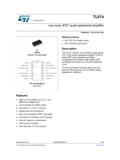
Low-noise JFET quad operational amplifier
www.st.comJul 07, 2008 · JFET input single operational amplifiers. Each of these JFET input operational amplifiers incorporates well matched, high-voltage JFET and bipolar transistors in a monolithic integrated circuit. The devices feature high slew rates, low input bias and offset currents, and low offset voltage temperature coefficient. Inverting Input 2
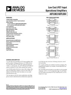
ADTL082/ADTL084 Low Cost JFET Input Operational …
www.analog.comThe ADTL082 and ADTL084 are JFET input amplifiers that provide industry-leading performance over TL08x devices. The ADTL082A and ADTL084A are improved versions of TL08x A, I, and Q grades. The ADTL082J and ADTL084J are industry alternatives to the TL08x standard and C grades. The ADTL08x family offers lower noise, offset voltage, offset