
Operational amplifier stability compensation methods for ...
Figure 9. Voltage follower configuration Figure 10. Closed loop gain measured for a voltage follower configuration Voltage Follower Configuration - Closed Loop Gain-40-30-20-10 0 10 20 1.E+03 1.E+04 1.E+05 1.E+06 1.E+07 Frequency (Hz) Gain (dB) Gain without CL Gain with CL = 550 pF TS507 : Vcc = 5 V Vicm = 2,5 V T = 25 °C RL = 10 kΩ Without ...
Download Operational amplifier stability compensation methods for ...

Information
Domain:
Source:
Link to this page:
Documents from same domain

Low-power dual operational amplifier - st.com
www.st.comFebruary 2016 DocID2471 Rev 17 1/24 This is information on a product in full production. www.st.com LM2904, LM2904A Low-power dual operational amplifier

AN3128 Application note - st.com
www.st.comJune 2011 Doc ID 16918 Rev 5 1/105 AN3128 Application note STM32 embedded graphic objects/touchscreen library Introduction This library is a firmware package which contains a collection of routines, data structures,

AN4767 Application note - st.com
www.st.comDocID028380 Rev 2 7/16 AN4767 Dual bank use cases 15 With dual bank, all the manipulation with the other bank is just another task of the main program.

AN3155 Application note - st.com
www.st.comOctober 2016 DocID17066 Rev 7 1/37 1 AN3155 Application note USART protocol used in the STM32 bootloader Introduction This application note describes the USART protocol used in the STM32 microcontroller

USB Power Delivery and Type-C - st.com
www.st.comUSB Type -C Overview USB Power Delivery specification introduces USB Type-C receptacle, plug and cable; they provide a smaller, thinner and more robust alternative to existing USB interconnect.

Datasheet - L78 - Positive voltage regulator ICs - …
www.st.comTO- 2 2 0 TO-2 2 0 F P DPAK D² PAK Features • Output current up to 1.5 A • Output voltages of 5; 6; 8; 8.5; 9; 12; 15; 18; 24 V • Thermal overload protection

AN2867 Application note - st.com
www.st.comMay 2017 DocID15287 Rev 11 1/43 1 AN2867 Application note Oscillator design guide for STM8AF/AL/S and STM32 microcontrollers Introduction Many designers know oscillators based on Pierce-Gate topology (hereinafter referred to as

AN4776 Application note - st.com
www.st.comMay 2017 DocID028459 Rev 2 1/73 1 AN4776 Application note General-purpose timer cookbook Introduction The timer peripheral is part of …

120-volt, 100-watt, DMOS audio amplifier with mute …
www.st.comSeptember 2010 Doc ID 6744 Rev 8 1/21 21 TDA7293 120-volt, 100-watt, DMOS audio amplifier with mute and standby Features Multipower BCD technology Very high operating voltage range (±50 V)

Electronic transformer for a 12V halogen lamp - …
www.st.comAPPLICATION NOTE AN528/0999 1/4 ELECTRONIC TRANSFORMER FOR A 12V HALOGEN LAMP by P. Fichera, R. Scollo 1. INTRODUCTION Lighting that uses halogen lamps is commonly found
Related documents

Lecture 20 Bipolar Junction Transistors (BJT): Part 4 ...
alan.ece.gatech.edu•Warning: Just like when a diode voltage exceeds a certain value, the non-linear behavior of the diode leads to distortion of the current/voltage curves (see previous lecture), if the inputs/outputs exceed certain limits, the full Ebers -Moll model ... Applying a voltage divider: BE /v.
Thevenin equivalent circuits - Iowa State University
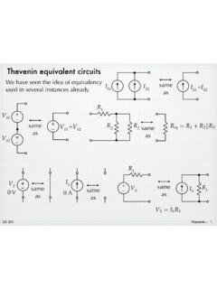
tuttle.merc.iastate.eduJun 10, 2014 · The open-circuit voltage / short-circuit current approach can be used to calculate the Thevenin equivalent for a known circuit. Consider the circuit from slide 4: + – V S R 1 R 2 I S 9V 6 mA 1.5 k! 3 k! Open-circuit voltage – Use whatever method you prefer. We’ll use node voltage in this case. + – V S R 1 R 2 I S v a + – v oc YRF= YD ...
Solving circuits directly using Laplace
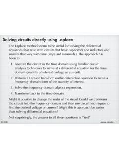
tuttle.merc.iastate.eduvoltage divider. = 1 sC R+ 1 sC +sL V i (s) V C (s) = Z C Z R +Z C +Z L V i (s) V C (s) = (1 1+sRC+s2LC)(V f s) = V f LC s(s2 +s R L + 1 LC) – + + – Z R V i (s) Z C V C (s) Z L Convert to the frequency domain. Z R = R

Lecture 19 - MIT
web.mit.eduVoltage divider at input: Voltage divider at output: Loaded voltage gain: v in=R vs Rin +Rs vout =RL Avovin Rout +RL vout vs = Rin Rin +RS Avo RL RL +Rout +-vin +-Avovin vout Rout +-Rin Rs vs +-RL unloaded circuit output loading input loading. 6.012 Spring 2007 Lecture 19 8 Small-signal voltage gain Avo: draw small-signal

Chapter 6: Voltage Regulator - Ajlon Tech
www.ajlontech.comA feedback voltage obtained from voltage divider R 1 and R 2 is applied to the op-amp’s non-inverting input and compared to the Zener voltage to control the drive current to the transistor. The current through resistor R S is thus controlled to drop a voltage across R S so that the output voltage is maintained.

Data Sheet ADP172 - Analog Devices
www.analog.comApr 21, 2021 · Subtract the current from the external resistor divider network in the case of adjustable voltage output (as with the ADP172) from the ground current measured. 2 Based on an end-point calculation using 1 mA and 300 mA loads.

VOLTAGE TRANSFORMERS
www.gegridsolutions.comwatts at rated secondary voltage when rated phase-to-ground voltage is impressed across the capacitance voltage divider. The rated burden of the device is the sum of the watt burdens that may be impressed on both secondary windings simultaneously. Adjustment capacitors are provided in the device for connecting in parallel with the