
Package Information : SOP8
SOP8 Package Information 7. Soldering conditions 7.1 Recommended temperature profile for reflow 7.2 Recommended condition for wave soldering Preheating temperature : 120 °C to 150 °C Preheating time : 60 sec MAX Soldering temperature : 260 °C ± 3 °C Soldering time : …
Download Package Information : SOP8

Information
Domain:
Source:
Link to this page:
Documents from same domain
SiC Power Devices and Modues Application Note
fscdn.rohm.com600V 400V 100V Si C D D D D G2GG 3ÿ G2GG H 9×3ÿ FÜ SiFÜ 8 æ GG ö G ì e Majority carrier device : High speed Minority carrier device : Low on-resistance, but low speed ・ Significant reduction in recovery loss ・ Downsizing of devices by increase in frequency Can be manufactured in this area, but little advantage over Si
Linear Regulator IC Series Linear Regulator 기초
fscdn.rohm.comLinear Regulator 는 기본적으로 입력, 출력, GND 핀으로 구성되며, 출력이 가변일 경우는 출력전압의 귀환이 필요 하기 때문에 귀환(Feedback)핀이 추가됩니다. (Figure 1) IN OUT FB GND V IN V O Figure 1. Linear Regulator 의 기본구성 Linear Regulator 내부회로의 개요는 Figure 2 …
Op-Amp/Comparator Application Note - Rohm
fscdn.rohm.comop-amp. Generally, an op-amp is composed of three stages: the input stage, the gain stage, and the output stage. The input stage is configured with a differential amplification stage that amplifies the differential voltage between the two terminals. In addition, it does not amplify the common-mode signal component (a condition where no ...
Efficiency of Buck Converter
fscdn.rohm.comEfficiency of Buck Converter Switching regulators are known as being highly efficient power sources. To further improve their efficiency, it is helpful to understand the basic mechanism of power loss. This application note explains power loss factors and methods for calculating them.
Snubber Circuit for Buck Converter IC : Power Management
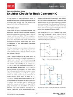
fscdn.rohm.comSnubber Circuit for Buck Converter IC AEK59-D1-0311-0 For example, when the input voltage VIN is 24 V and the switching frequency fSW is 1 MHz, 2 Ë Ì Ç » L680 pF H24 6 H1 MHz L0.39 W the generated consumption power of 0.39 W requires a 6432 size resistor (2512 in inches) with a rated power of 1 W.
ISO 26262: Functional Safety Standard for Modern Road …
fscdn.rohm.comIntrinsic safety is a method for ensuring safety by removing the causes of danger. Functional safety, on the other hand, is a method of reducing risks to an acceptable level to ensure safety ... verification, prototyping, and evaluation are clarified, with reviews performed at each stage. It is also necessary to manage the documents created at
Calculation of Power Loss (Synchronous) : Power Management
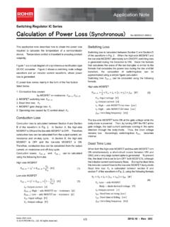
fscdn.rohm.comCalculation of Power Loss (Synchronous) This application note describes how to obtain the power loss required to calculate the temperature of a semiconductor device. Temperature control is important to ensuring product reliability. Figure 1 is a circuit diagram of a synchronous rectification type DC/DC converter. Figure 2 shows a switching node ...
Inductor Calculation for Buck Converter IC
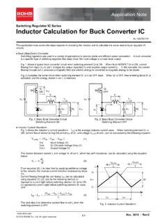
fscdn.rohm.comInductor Calculation of Buck Converter Current-difference between max. and min. (ILP-ILT) is as follows: IN SW D SW IN SW OUT D OUT LP LT V V V L f V V V V V I I (15) Equations (13) and (15) show that large inductance L and high switching frequency will reduce maximum current (ILP)and current difference between max. and min. (ILP-ILT).
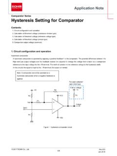
Hysteresis Setting for Comparator - Rohm
fscdn.rohm.comprovided only to illustrate the standard usage and operations of the Products. The peripheral conditions must be taken into account when designing circuits for mass production. The technical information specified herein is intended only to show the typical functions of and examples of application circuits for the Products.
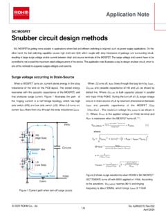
Snubber circuit design methods - Rohm
fscdn.rohm.comis bulk capacitor placed in parallel with input HVdc-PGND. During the turn off of LS, surge voltage occurs in drain-source of LS by resonant phenomenon between L MAIN and parasitic capacitance of the MOSFET C OSS ( C DS + DG). The maximum voltage V DS_SURGE is as shown in (1). Where V HVDC is the applied voltage on HVdc terminal and R OFF
Related documents
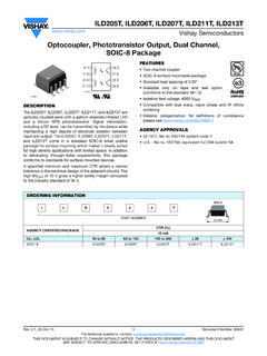
Optocoupler, Phototransistor Output, Dual Channel, SOIC-8 ...
www.vishay.comTotal package dissipation ambient (2 LEDs and 2 detectors, 2 channels) Ptot 350 mW Storage temperature Tstg-55 to +150 °C Operating temperature Tamb-55 to +100 °C Soldering time from 260 °C (1) Tsld 10 s ELECTRICAL CHARACTERISTICS (Tamb = 25 °C, unless otherwise specified) PARAMETER TEST CONDITION SYMBOL MIN. TYP. MAX. UNIT INPUT
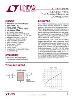
LT1963A - 1.5A, Low Noise, Fast Transient Response LDO ...
www.analog.comlead based finish tape and reel part marking* package description temperature range LT1963AET-1.5 LT1963AET-1.5#TR LT1963AET-1.5 5-Lead Plastic TO-220 –40°C to 125°C LT1963AET-1.8 LT1963AET-1.8#TR LT1963AET-1.8 5-Lead Plastic TO-220 –40°C to 125°C

2.7V 4-Channel/8-Channel 10-Bit A/D Converters with SPI ...
cdn-shop.adafruit.comJan 02, 2008 · Soldering temperature of leads (10 seconds).....+300°C ESD Protection On All Pins (HBM).....≥ 4kV † Notice: Stresses above those listed under “Absolute Maximum Ratings” may cause permanent damage to the device. This is a stress rati ng only and functional operation of ... Thermal Package Resistances

PACKAGE INFORMATION 1. PACKAGE CLASSIFICATIONS
img.ozdisan.comPACKAGE INFORMATION 1. PACKAGE CLASSIFICATIONS 1 1. PACKAGE CLASSIFICATIONS 1.1 Packaging Trends In recent years, marked advances have been made in the electronics field. One such advance has been the progression from vacuum tubes to transistors and finally, to ICs. ICs themselves have been more highly integrated into LSIs, …

SOT23 - NXP
www.nxp.comWave soldering footprint SOT023_fw Package life cycle status REL Major version date 18-9-2008 Minor version date 6-7-2012 Security status COMPANY PUBLIC Modified date 28-11-2012 Issue date 16-3-2006 Web publication date 28-11-2012 Initial web publication date 11-3-2011 Customer specific indicator N
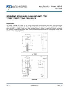
MOUNTING AND HANDLING GUIDELINES FOR …
aosmd.comthe time-temperature specification of the package is not exceeded in the soldering operation. References 1. Sanjay Havanur, Application Note: AN101-1 , June, 2007 This document contains preliminary data; supplementary data may be published at a later date. Alpha and Omega Semiconductor reserves the right to make changes at any time without notice.

SMA - Diodes Incorporated
www.diodes.comSurface Mount Package Case Material: Molded Plastic, UL Flammability Rating 94V-0 Terminals: Finish - Matte Tin Plated Leads, Solderable per MIL-STD-202, Method 208 Weight: 0.064 grams (Approximate) Max Soldering Temperature +260°C for 30 secs as per JEDEC J-STD-020 Package View Package Outline Dimensions SMA

SMB - Diodes Incorporated
www.diodes.comSurface Mount Package Case Material: Molded Plastic, UL Flammability Rating 94V-0 Terminals: Finish - Matte Tin Plated Leads, Solderable per MIL-STD-202, Method 208 Weight: 0.096 grams (Approximate) Max Soldering Temperature +260°C for 30 secs as per JEDEC J-STD-020 Package View Package Outline Dimensions SMB SMB

Package dimensions MSOP, SSOP, TSSOP-A2 - iC-Haus
www.ichaus.deFor additional information on component handling, preconditioning and soldering conditions, refer to the relevant iC-Haus customer information files, available separately. iC-Haus Application Guide More Package Info. Title: Package dimensions MSOP, SSOP, TSSOP-A2.indd Created Date: 8/4/2006 1:07:11 PM ...