PIC12F629/675 Data Sheet
AN1 AN A/D Channel 1 input CIN- AN Comparator input VREF AN External voltage reference ICSPCLK ST Serial programming clock GP2/AN2/T0CKI/INT/COUT GP2 ST CMOS Bi-directional I/O w/ programmable pull-up and interrupt-on-change AN2 AN A/D Channel 2 input T0CKI ST TMR0 clock input INT ST External interrupt COUT CMOS Comparator output GP3/MCLR/VPP
Download PIC12F629/675 Data Sheet

Information
Domain:
Source:
Link to this page:
Documents from same domain

Power Factor Correction in Power Conversion …
ww1.microchip.com© 2007 Microchip Technology Inc. DS01106A-page 2 AN1106 FIGURE 1: CURRENT WAVEFORMS WITH AND WITHOUT PFC These waveforms illustrate that …

2.7V to 5.5V Single Supply CMOS Op Amp
ww1.microchip.comMCP601/1R/2/3/4 DS21314G-page 2 © 2007 Microchip Technology Inc. 1.0 ELECTRICAL CHARACTERISTICS Absolute Maximum Ratings † VDD –VSS.....7.0V

Data Encryption Routines for PIC24 and dsPIC Device
ww1.microchip.com© 2006 Microchip Technology Inc. DS01044A-page 1 AN1044 INTRODUCTION Currently, there are three data encryption standards approved …

Using SAM-BA for Linux on SAMA5D3 Xplained
ww1.microchip.comAN-8995 – Using SAM-BA for Linux on SAMA5D3 Xplained: 42328A−06/2014 Page 5 of 19 2. Setup With Ubuntu distributions, a user has to be member of the dialout group to access serial devices like

MCP6021/1R/2/3/4 - Rail-to-Rail Input/Output, 10 …
ww1.microchip.com2001-2017 Microchip Technology Inc. DS20001685E-page 1 MCP6021/1R/2/3/4 Features • Rail-to-Rail Input/Output • Wide Bandwidth: 10 MHz (typical)

Low Quiescent Current LDO - Microchip Technology
ww1.microchip.com2005-2016 Microchip Technology Inc. DS20001826D-page 1 MCP1700 Features: • 1.6 µA Typical Quiescent Current • Input Operating Voltage Range: 2.3V to 6.0V

MCP1703 250 mA, 16V, Low Quiescent Current
ww1.microchip.com2010 Microchip Technology Inc. DS22049E-page 1 MCP1703 Features: • 2.0 µA Typical Quiescent Current • Input Operating Voltage Range: 2.7V to16.0V

MTCH6102 Low-Power Projected Capacitive Touch …
ww1.microchip.com2014 Microchip Technology Inc. DS40001750A-page 1 Description: Microchip’s MTCH6102 is a turnkey projected capacitive touch controller that simplifies adding

PIC32 GUI Development Board with Projected …
ww1.microchip.comPIC32 GUI Development Board with Projected Capacitance (PCAP) Touch Information Sheet Microchip Technology Inc.

RN4020 Bluetooth Low Energy Module User’s Guide
ww1.microchip.comRN4020 BLUETOOTH LOW ENERGY MODULE USER’S GUIDE 2014 Microchip Technology Inc. DS70005191B-page 7 Preface INTRODUCTION This chapter contains general information that will be useful to know before using the
Related documents
Chapter 4 Low-Power VLSI DesignPower VLSI Design
www.ee.ncu.edu.tw4/4 1 0 t iti l k4/4 = 1.0 transition per clock • Gray-code counter is more power efficient.code counter is more power efficient. G. K. Yeap, Practical Low Power Digital VLSI Design, Boston: Kluwer Academic Publishers (now Springer) 1998 National Central University EE4012VLSI Design 30 Kluwer Academic Publishers (now Springer), 1998.

LM339 - Single Supply Quad Comparators
www.onsemi.comthe comparator will provide a proper output state. Refer to the Maximum Ratings table for safe operating area. ... CMOS TTL 1/4 MC14001 1/4 MC7400 +15 +5.0 100 10 RS = Source Resistance R1 RS T1 = T2 = 0.69 RC f 7.2 C( F) ... It is good design practice to ground all unused input pins. Differential input voltages may be larger than supply
Analog Integrated Circuit Design 2nd Edition
www.d.umn.edu10.1.1 Input offset and noise The input offset voltage of a comparator is the input voltage at which its output changes from one logic level to the other. It may be caused by device mismatch or may be inherent to the design of a comparator. Random circuit noise can cause the output to change from one logic level to the other, even

Examples of Solved Problems for Chapter3,5,6,7,and8
www.eecg.utoronto.caThen, X ≤ Y is detected by Z +(N ⊕V) = 1. The last two cases are just simple inverses: X>Yif Z +(N ⊕V)=1andX ≥ Y if N ⊕V =1. Figure 5.43. A comparator circuit. Example 6.25 Problem: Implement the function f(w1,w2,w3)= m(0,1,3,4,6,7) by …

2-Bit Magnitude Comparator Design Using Different Logic …
www.ijesi.org3. 2-BIT MAGNITUDE COMPARATOR DESIGN USING DIFFERENT LOGIC STYLES 3.1. Using CMOS Logic Style Fig.3 (a) represents symbol of CMOS Inverter. It consists of one NMOS & one PMOS transistor. If input A=0 (logic low) then both gates are at zero potential & PMOS is ON & provide low impedance path from V DD to output (Y).
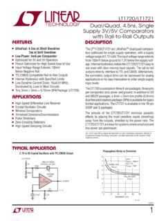
LT1720/LT1721 - Dual/Quad, 4.5ns, Single Supply 3V/5V ...
www.analog.comLT1720/LT1721 3 17201fc ELECTRICAL CHARACTERISTICS SYMBOL PARAMETER CONDITIONS MIN TYP MAX UNITS VCC Supply Voltage l 2.7 6 V ICC Supply Current (Per Comparator) VCC = 5V VCC = 3V l l 4 3.5 7 6 mA mA VCMR Common Mode Voltage Range (Note 2) l –0.1 VCC – 1.2 V VTRIP+ Input Trip Points (Note 3) l –2.0 –3.0 5.5 6.5 mV mV …
CMOS Comparator Design
www.eecis.udel.eduVishal Saxena -1- CMOS Comparator Design Extra Slides Vishal Saxena, Boise State University (vishalsaxena@boisestate.edu) Vishal Saxena -2- Comparator Design Considerations
TUTORIAL - Analog Devices
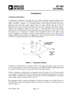
www.analog.comRev.A, 09/2011, WK Page 1 of 7 MT-083 TUTORIAL Comparators . COMPARATOR BASICS . A comparator is similar to an op amp. It has two inputs, inverting and non-inverting and an output (see Figure 1). But it is specifically designed to compare the voltages between its two inputs. Therefore it operates in a non-linear fashion. The comparator operates ...

Design and Simulation of CMOS Schmitt Trigger
ijiset.comof Schmitt trigger is using CMOS technology in different foundry. Then, post-layout simulation of Schmitt trigger is done in Microwind 3.1 using90nm, 65nm and 45 nm CMOS technology. The design is implemented using DSCH software to calculate area and power consumption.