
The Bandgap Reference
Low-Voltage Bandgap References The basic bandgap expression, VV BE +17.,2 T takes on a value of about 1.25 V at T = 300K, defying direct implementation in today’s low-voltage technologies. We describe one low-voltage example and refer the reader to [10] and [11] for others. For a low-voltage bandgap reference to have a zero TC, it must produce an
Download The Bandgap Reference

Information
Domain:
Source:
Link to this page:
Documents from same domain
Fundamentals of Chemical Reactor Theory1 - …
www.seas.ucla.edu1 UNIVERSITY OF CALIFORNIA, LOS ANGELES Civil & Environmental Engineering Department Fundamentals of Chemical Reactor Theory Michael K. Stenstrom
Introduction to Switched-Capacitor Circuits
www.seas.ucla.eduChapter 12. Introduction to Switched-Capacitor Circuits 398 Vout Vin C1 Vout V C C1 2 AB AB in0 (a) (b) Vin VA Vin0 t0 t Vin0 C1 C2 (c) Vout Figure 12.5. Circuit of Fig. 12.4 in (a) sampling mode, (b) amplification mode.

Noise in RF Design - Engineering
www.seas.ucla.eduEE215C B. Razavi Win. 13 HO #2 17 Example Noise Figure At high frequencies, it becomes difficult to measure the input-referred noise …
CMOS technology characterization for analog and …
www.seas.ucla.eduCMOS Technology Characterization for Analog and RF Design Behzad Razavi, Member, IEEE Abstract— The design of analog and radio-frequency (RF) circuits in CMOS technology becomes increasingly more difficult as device modeling faces new challenges in deep submicrometer processes and emerging circuit applications. The …

Analog Integrated Circuit Design - Engineering
www.seas.ucla.eduEE 215A HO#1 Fall 2014 Analog Integrated Circuit Design Instructor: Behzad Razavi 56-147D, Eng. IV
International Journal of Heat and Mass Transfer - …
www.seas.ucla.eduS;T refers to heat of mixing due to temperature gradient 638 A. d’Entremont, L. Pilon/International Journal of Heat and Mass Transfer 75 (2014) 637–649 depends on the ion concentration distribution and vice versa.

Seismic Code Requirements - Engineering
www.seas.ucla.eduBuilding Response Analysis zIn general, three types of analyses are done to design buildings subjected to earthquakes – Response History Analysis zLinear or nonlinear approach to calculate time varying responses (P, M, V, δ) – Response Spectrum Analysis zLinear approach to calculate modal responses (peak values) and combine modal responses
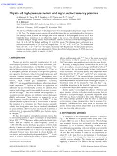
Physics of high-pressure helium and argon radio-frequency ...
www.seas.ucla.eduThe physics of helium and argon rf discharges have been investigated in the pressure range from 50 to 760 Torr. The plasma source consists of metal electrodes that are perforated to allow the gas to

Fall 14 HO #8 - School of Engineering and Applied Science
www.seas.ucla.eduEE215A B. Razavi Fall 14 HO #8 1 Differential Amplifiers Differential & Single-Ended Operation - A single-ended signal is taken with

L.Vandenberghe ECE133A(Fall2018) 5.Orthogonalmatrices
www.seas.ucla.eduProof thesquareddistanceofb toanarbitrarypointAx inrange„A”is kAx bk2 = kA„x xˆ”+ Axˆ bk2 (wherexˆ = ATb) = kA„x xˆ”k2 + kAxˆ bk2 +2„x xˆ”TAT„Axˆ b” = kA„x xˆ”k2 + kAxˆ bk2 = kx xˆk2 + kAxˆ bk2 kAxˆ bk2 withequalityonlyifx = xˆ line3followsbecauseAT„Axˆ b”= xˆ ATb = 0 line4followsfromATA = I Orthogonalmatrices 5.18
Related documents
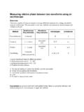
Measuring relative phase between two waveforms using an ...
eeshop.unl.edudc offset automatically. This method was developed using the Tektronix 2012B oscilloscope. Waveforms: • Sinusoidal • Common frequency Method: • Display the two traces in voltage v. time mode, along with the product trace in voltage2 v. time mode. Use ac coupling. • Fit the traces in the screen vertically.
Current Sensing Circuit Concepts and Fundamentals
ww1.microchip.comHowever, the voltage drop across the sensing resistor may become low enough to be comparable to the input offset voltage of subsequent analog conditioning circuit, which would compromise the measurement accuracy. In addition, the current sensing resistor’s inherent inductance must be low, if the measured current has a large high-frequency ...
Ultralow Power, Low Distortion, Fully Differential ADC ...
www.analog.com0.35 mV maximum offset voltage Balanced outputs Settling time to 0.1%: 34 ns Rail-to-rail output: −V S + 0.1 V to +V S − 0.1 V Adjustable output common-mode voltage Flexible power supplies: 3 V to 7 V (LFCSP) Disable pin to reduce power consumption ADA4940-1 is available in LFCSP and SOIC packages APPLICATIONS Low power PulSAR®/SAR ADC drivers

Precision, Low Cost, High Speed BiFET Dual Op Amp Data ...
www.analog.comand 100% testing guarantee a low input offset voltage (3 mV maximum, J grade). Input offset voltage is specified in the warmed-up condition. 3. Together with precision dc performance, the AD712 offers excellent dynamic response. It settles to ±0.01% in 1 μs and has a minimum slew rate of 16 V/μs. Thus, this device is

LM358 - Diodes Incorporated
www.diodes.com• Low input offset voltage: 2mV • Wide power supply range: o Single supply: 3V to 32V o Dual supplies: ±1.5V to ±16V • Large output voltage swing: 0V to V+ - 1.5V • SOP-8L packaging • “Green” Molding Compound (No Br, Sb) • Lead Free Finish/ RoHS Compliant (Note 1) Pin Assignments ...