
Transphrom–氮化镓FET(HEMT)
Transphrom–氮化镓FET(HEMT) www.transphormusa.com, HEMT: High Electron Mobility Transistor 氮化镓MOSFET (600VDC, 能承受周期为1uS,100nS的连续的方波,保证750V) Part Number Package Voltage (V) Current (A) Ron(Ohm) Description TPH3245ED下载 QFN 5*6 750 6 0.5 背部金属接D极 TPH3002LD下载 QFN 8*8 750 9 0.29 背部金属 ...
Download Transphrom–氮化镓FET(HEMT)

Information
Domain:
Source:
Link to this page:
Documents from same domain

CENELEC - dianyuan.com
www.dianyuan.comEUROPEAN STANDARD EN 61547 NORME EUROPÉENNE EUROPÄISCHE NORM August 2009 CENELEC European Committee for Electrotechnical Standardization Comité Européen de Normalisation Electrotechnique

LLC设计步骤 - dianyuan.com
www.dianyuan.comLLC设计步骤 ¾LLC的基本原理 ¾LLC的设计方法 ¾LLC的几个问题 www.21dianyuan.com 版权:世纪电源网|作者:郭春明,未经允许不得转载!

基于ZigBee的无线数据采集系统的设计
www.dianyuan.com速率为250kbps。CC2430仅需添加少量的外围元件 就可以完成ZIGBEE通信功能的硬件实现。 C8051F020是Cygnal公司推出的基于CIP-51内 核的SOt2芯片,在硬件设计上它采用流水线结构, 机器周期由标准的12个系统时钟周期降到1个,因 此指令执行速度有很大的提高。具有64个I/O引

Electromagnetic compatibility of multimedia equipment ...
www.dianyuan.comANSI C63.5 2006 American National Standard (for) Electromagnetic Compatibility - Radiated Emission Measurements in Electromagnetic Interference (EMI) Control - Calibration of Antennas (9 kHz to 40 GHz) - - IEEE 802.3 - IEEE Standard for Information technology - Specific requirements - Part 3: Carrier Sense Multiple Access with

基于DSP双闭环控制的单相逆变电源设计与实现
www.dianyuan.com逆变电源spwm调制和闭环控制主要由中断程序 完成。中断程序流程如图5所示。进入中断后,首 先对电压和电流进行采样,将采到的数据进行调 理,计算电压的误差,经过pi调节后作为电流内环 的给定值,然后计算电流的误差值,经过比例调节 后生成spwm信号。

基于LabVIEW的数据采集高级编程 - dianyuan.com
www.dianyuan.comNI公司在全球数据采集产品市场中的地位 31.6% 9.4% 8.8% 7.5% 6.8% 4.8% 0% 50% 100% National Instruments Vendor #1 Vendor #2 Vendor #3 Vendor #4 Vendor #5 Figure 2.7 presents the company market share by revenues in the data acquisition boards, modules & software (not including interface-

LED照明灯具驱动电路 设计技术 - dianyuan.com
www.dianyuan.compt4115用于mr16快速推广模式 可用于生产 demo pcb光板 +样片 200-1k 小批量生产 2-30k 批量生产 推广流程 推广周期 第1周第第2周 第3/4周 5/6周 推广材料成本 demo rmb3.20 pcbx20 rmb6.00 pt4115x20 rmb32.00 ss14x5 0.45 cinx1 0.10 rsx1 0.05 lx1 0.60 pcbx1 0.30 pt4115 1.60

南京微盟电子有限公司 - dianyuan.com
www.dianyuan.como On-card switching regulators Positive to negative ... SOT23-5 ME6203 ~40 V 100 mA 3.0-5.0V ±2% 3uA 50dB 1100mV (@50mA) TO92/SOT89-3 Applications: Mobil ephonID C ordl ss Rad icmmun at on equ pment Wireless communication equipment Electronic Balance Toys Reference voltage Battery powered equipment Ammeter Portable games Reference voltage ...
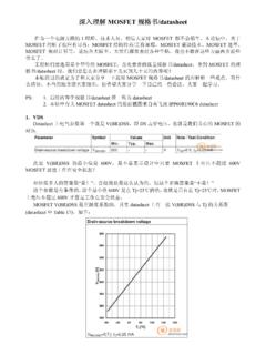
深入理解 MOSFET /datasheet - dianyuan.com
www.dianyuan.com5. Ciss, Coss, Crss MOSFET带寄生电容的等效模型 Ciss=Cgd+Cgs, Coss=Cgd+Cds, Crss=Cgd Ciss, Coss, Crss的容值都是随着VDS电压改变而改变的,如下图: 在LLC 拓扑中,减小死区时间可以提高效率,但过小的死区时间会导致无法实现ZVS。因此
Related documents

NCP51820 - High Speed Half-Bridge Driver for GaN Power ...
www.onsemi.comDriver for GaN Power Switches NCP51820 The NCP51820 high−speed, gate driver is designed to meet the stringent requirements of driving enhancement mode (e−mode), high electron mobility transistor (HEMT) and gate injection transistor (GIT), gallium nitrade (GaN) power switches in off−line, half−bridge power topologies.
Gallium Nitride (GaN) versus Silicon Carbide (SiC)
www.richardsonrfpd.comGallium Nitride (GaN). These material properties have a major influence on the fundamental performance characteristics of the devices. Both SiC and GaN have material properties superior to Si for RF and Switching Power devices. The high critical field of both GaN and SiC compared to Si is a property which allows these

Insights into gallium oxide growth
data.angel.digitalMar 01, 2022 · the INN40W08, a 40 V bi-directional GaN-on-silicon enhancement mode HEMT for mobile devices, including laptops and cellular phones. The INN40W08 HEMT has been developed using the company’s InnoGaN technology. Denis Marcon, general manager of Innoscience Europe and marketing manager for the USA and Europe, remarked: “GaN …

GaN HEMTを用いた携帯電話基地局向け 広帯域・高出力・高 …
sei.co.jp(GaN HEMT※1: Gallium Nitride High Electron Mobility Transistor)の研究および開発を2000年から進め、2006 ... power wideband asymmetric Doherty amplifier using the devices are also described. The transistor has a pair of 180 W GaN dies. The internal matching circuit is designed with a high-dielectric substrate so that it can ...

HEMT - Fujitsu
www.fujitsu.comGaN HEMT I ds V ds 0 0 ドレイン電圧 V ds ( V ) ドレイン電流 I ds ( A ) (b)GaN HEMTとSJ Si MOSFETのパルス応答特性 スイッチング損失 スイッチング損失 表-2 スイッチング特性比較 GaN HEMT Si MOSFET オン時間(ns) 7.0 41.5 オフ時間(ns) 7.5 30.5 オン損失(µJ) 5.6 45.4 ...

GaN系半導体デバイスの技術開発課題と ... - JST
www.jst.go.jpThe GaN devices are expected to be developed for various applications in near future because of the attractive physical properties of GaN including wide bandgap, optical properties and electrical properties. In this report, the current status of the researches and developments of laser diodes, high-frequency ... 5.1 横型HEMT構造と縦型 ...