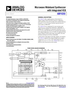
Transcription of Integrated Synthesizer and VCO Data Sheet ADF4360-7
1 Integrated Synthesizer and VCO Data Sheet ADF4360-7 Rev. F Document Feedback Information furnished by Analog Devices is believed to be accurate and reliable. However, no re-sponsibility is assumed by Analog Devices for its use, nor for any infringements of patents or other rights of third parties that may result from its use. Specifications subject to change without notice. No license is granted by implication or otherwise under any patent or patent rights of Analog Devices. Trademarks and registered trademarks are the property of their respective owners. One Technology Way, Box 9106, Norwood, MA 02062-9106, Tel: 2004 2018 Analog Devices, Inc. All rights reserved. Technical Support FEATURES Output frequency range: 350 MHz to 1800 MHz Divide-by-2 output V to V power supply V logic compatibility Integer-N Synthesizer Programmable dual-modulus prescaler 8/9, 16/17 Programmable output power level 3-wire serial interface Analog and digital lock detect Hardware and software power-down mode APPLICATIONS Wireless handsets (DECT, GSM, PCS, DCS, WCDMA) Test equipment Wireless LANs CATV equipment GENERAL DESCRIPTION The ADF4360-7 is an Integrated integer-N Synthesizer and voltage controlled oscillator (VCO).
2 The ADF4360-7 center frequency is set by external inductors. This allows a frequency range of between 350 MHz to 1800 MHz. In addition, a divide-by-2 option is available, whereby the user receives an RF output of between 175 MHz and 900 MHz. Control of all the on-chip registers is through a simple 3-wire interface. The device operates with a power supply ranging from V to V and can be powered down when not in use. FUNCTIONAL BLOCK DIAGRAM MUXOUTCPVVCOREFINCLKDATALEAVDDDVDDRSETAG NDDGNDCPGNDCEVTUNECCCNL1L2 RFOUTARFOUTBVCOCOREPHASECOMPARATORMUTEDI VSEL = 2 DIVSEL = 1N = (BP + A)LOADLOADCHARGEPUMPOUTPUTSTAGEMULTIPLEX ERINTEGERREGISTER13-BIT BCOUNTER14-BIT RCOUNTER24-BITFUNCTIONLATCH24-BITDATA REGISTER5-BIT ACOUNTERPRESCALERP/P+1 MULTIPLEXERLOCKDETECT 2 adf4360 -704441-001 Figure 1. ADF4360-7 Data Sheet Rev. F | Page 2 of 25 TABLE OF CONTENTS Features .. 1 Applications .. 1 General Description.
3 1 Functional Block Diagram .. 1 Revision History .. 2 Specifications .. 3 Timing Characteristics .. 5 Absolute Maximum Ratings .. 6 Transistor Count .. 6 ESD Caution .. 6 Pin Configuration and Function Descriptions .. 7 Typical Performance Characteristics .. 8 Circuit Description .. 10 Reference Input Section .. 10 Prescaler (P/P + 1) .. 10 A and B Counters .. 10 R Counter .. 10 PFD and Charge Pump .. 10 MUXOUT and Lock Detect .. 11 Input Shift Register .. 11 VCO .. 11 Output Stage .. 12 Latch Structure .. 13 Power-Up .. 17 Control Latch .. 19 N Counter Latch .. 20 R Counter Latch .. 20 Applications Information .. 21 Frequency Generator .. 21 Choosing the Correct Inductance Value .. 22 Choosing the Appropriate PFD Frequency .. 22 Fixed Frequency LO .. 22 Interfacing .. 23 PCB Design Guidelines for Chip Scale 23 Output Matching .. 24 Outline Dimensions .. 25 Ordering Guide .. 25 REVISION HISTORY 9/2018 Rev.
4 E to Rev. F Added Choosing the Appropriate PFD Frequency Section .. 22 4/2016 Rev. D to Rev. E Changed adf4360 Family to ADF4360-7 , ADSP-21xx to ADSP-2181, and EV- adf4360 -xEB1 to Throughout Changes to Figure 3 .. 7 Updated Outline Dimensions .. 25 Changes to Ordering Guide .. 25 3/2013 Rev. C to Rev. D Changes to Prescaler (P/P + 1) Section .. 10 11/2012 Rev. B to Rev. C Changes to Table 3 .. 6 Updated Outline Dimensions .. 25 2/2012 Rev. A to Rev. B Changes to Figure 3 and Ta b l e 4 .. 8 Changes to Output Matching 24 Updated Outline Dimensions .. 25 Changes to Ordering Guide .. 25 11/2004 Rev. 0 to Rev. A Updated Format .. Universal Changes to General Description .. 1 Changes to Specifications .. 3 Changes to the Reference Input 10 Changes to Power-Up Section .. 17 Added Table 10 .. 17 Added Figure 22 .. 17 Updated Outline Dimensions .. 25 2/2004 Revision 0: Initial Version Data Sheet ADF4360-7 Rev.
5 F | Page 3 of 25 SPECIFICATIONS1 AVDD = DVDD = VVCO = V 10%; AGND = DGND = 0 V; TA = TMIN to TMAX, unless otherwise noted. Table 1. Parameter B Version Unit Test Conditions/Comments REFIN CHARACTERISTICS REFIN Input Frequency 10/250 MHz min/max For f < 10 MHz, use a dc-coupled CMOS-compatible square wave, slew rate > 21 V/ s. REFIN Input Sensitivity V p-p min/max AC-coupled. 0 to AVDD V max CMOS compatible. REFIN Input Capacitance pF max REFIN Input Current 60 A max PHASE DETECTOR Phase Detector Frequency2 8 MHz max CHARGE PUMP ICP Sink/Source3 With RSET = k . High Value mA typ Low Value mA typ RSET Range k ICP Three-State Leakage Current nA typ Sink and Source Current Matching 2 % typ V VCP V. ICP vs. VCP % typ V VCP V. ICP vs. Temperature 2 % typ VCP = V. LOGIC INPUTS VINH, Input High Voltage V min VINL, Input Low Voltage V max IINH/IINL, Input Current 1 A max CIN, Input Capacitance pF max LOGIC OUTPUTS VOH, Output High Voltage DVDD V min CMOS output chosen.
6 IOH, Output High Current 500 A max VOL, Output Low Voltage V max IOL = 500 A. POWER SUPPLIES AVDD V min/V max DVDD AVDD VVCO AVDD AIDD4 10 mA typ DIDD4 mA typ IVCO4, 5 mA typ ICORE = 5 mA. IRFOUT4 to mA typ RF output stage is programmable. Low Power Sleep Mode 7 A typ ADF4360-7 Data Sheet Rev. F | Page 4 of 25 Parameter B Version Unit Test Conditions/Comments RF OUTPUT CHARACTERISTICS5 Maximum VCO Output Frequency 1800 MHz ICORE = 5 mA. Depending on L. See the Choosing the Correct Inductance Value section. Minimum VCO Output Frequency 350 MHz VCO Output Frequency 490/585 MHz min/max L1, L2 = 13 nH. See the Choosing the Correct Inductance Value section for other frequency values. VCO Frequency Range Ratio FMAX/FMIN VCO Sensitivity 12 MHz/V typ L1, L2 = 13 nH. See the Choosing the Correct Inductance Value section for other sensitivity values.
7 Lock Time6 400 s typ To within 10 Hz of final frequency. Frequency Pushing (Open Loop) 6 MHz/V typ Frequency Pulling (Open Loop) 15 kHz typ Into VSWR load. Harmonic Content (Second) 19 dBc typ Harmonic Content (Third) 9 dBc typ Output Power5, 7 14/ 5 dBm typ Programmable in 3 dB steps. See Table 7. Output Power Variation 3 dB typ For tuned loads, see Output Matching section. VCO Tuning Range V min/max NOISE CHARACTERISTIC5 VCO Phase-Noise Performance8 116 dBc/Hz typ At 100 kHz offset from carrier. 138 dBc/Hz typ At 1 MHz offset from carrier. 144 dBc/Hz typ At 3 MHz offset from carrier. 148 dBc/Hz typ At 10 MHz offset from carrier. Synthesizer Phase-Noise Floor9 172 dBc/Hz typ At 25 kHz PFD frequency. 163 dBc/Hz typ At 200 kHz PFD frequency. 147 dBc/Hz typ At 8 MHz PFD frequency. In-Band Phase Noise10, 11 92 dBc/Hz typ At 1 kHz offset from carrier.
8 RMS Integrated Phase Error12 Degrees typ 100 Hz to 100 kHz. Spurious Signals due to PFD Fre-quency11, 13 70 dBc typ Level of Unlocked Signal with MTLD Enabled 44 dBm typ 1 Operating temperature range is 40 C to +85 C. 2 Guaranteed by design. Sample tested to ensure compliance. 3 ICP is internally modified to maintain constant loop gain over the frequency range. 4 TA = 25 C; AVDD = DVDD = VVCO = V; P = 32. 5 Unless otherwise stated, these characteristics are guaranteed for VCO core power = 5 mA. L1, L2 = 13 nH, 470 resistors to GND in parallel with L1, L2. 6 Jumping from 490 MHz to 585 MHz. PFD frequency = 200 kHz; loop bandwidth = 10 kHz. 7 Using 50 resistors to VVCO, into a 50 load. For tuned loads, see the Output Matching section. 8 The noise of the VCO is measured in open-loop conditions. 9 The Synthesizer phase-noise floor is estimated by measuring the in-band phase noise at the output of the VCO and subtracting 20 log N (where N is the N divider value).
9 10 The phase noise is measured with the EV- adf4360 -7EB1Z Evaluation Board and the HP 8562E Spectrum Analyzer. The Spectrum Analyzer provides the REFIN for the Synthesizer ; offset frequency = 1 kHz. 11 fREFIN = 10 MHz; fPFD = 200 kHz; N = 2500; loop B/W = 10 kHz. 12 fREFIN = 10 MHz; fPFD = 1 MHz; N = 500; loop B/W = 25 kHz. 13 The spurious signals are measured with the EV- adf4360 -7EB1Z Evaluation Board and the HP 8562E Spectrum Analyzer. The Spectrum Analyzer provides the REFIN for the Synthesizer ; fREFOUT = 10 MHz at 0 dBm. Data Sheet ADF4360-7 Rev. F | Page 5 of 25 TIMING CHARACTERISTICS1 AVDD = DVDD = VVCO = V 10%; AGND = DGND = 0 V; V and 3 V logic levels used; TA = TMIN to TMAX, unless otherwise noted. Table 2. Parameter Limit at TMIN to TMAX (B Version) Unit Test Conditions/Comments t1 20 ns min LE Setup Time t2 10 ns min DATA to CLOCK Setup Time t3 10 ns min DATA to CLOCK Hold Time t4 25 ns min CLOCK High Duration t5 25 ns min CLOCK Low Duration t6 10 ns min CLOCK to LE Setup Time t7 20 ns min LE Pulse Width 1 Refer to the Power-Up section for the recommended power-up procedure for this device.
10 CLOCKDATALELEDB23 (MSB)DB22DB2DB1(CONTROL BIT C2)DB0 (LSB)(CONTROL BIT C1)t1t2t3t7t6t4t504441-002 Figure 2. Timing Diagram ADF4360-7 Data Sheet Rev. F | Page 6 of 25 ABSOLUTE MAXIMUM RATINGS TA = 25 C, unless otherwise noted. Table 3. Parameter Rating AVDD to GND1 V to + V AVDD to DVDD V to + V VVCO to GND V to + V VVCO to AVDD V to + V Digital I/O Voltage to GND V to VDD + V Analog I/O Voltage to GND V to VDD + V REFIN to GND V to VDD + V Operating Temperature Maximum Junction Temperature 150 C CSP JA Thermal Impedance Paddle Soldered 50 C/W Paddle Not Soldered 88 C/W Peak Soldering Reflow Temperature 260 C 1 GND = AGND = DGND = 0 V. Stresses at or above those listed under Absolute Maximum Rat-ings may cause permanent damage to the product. This is a stress rating only; functional operation of the product at these or any other conditions above those indicated in the operational section of this specification is not implied.