Transcription of LTM8026: 36VIN, 5A CVCC Step-Down µModule …
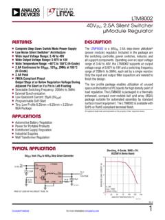
1 LTM8026. 36 VIN, 5A CVCC Step-Down Module Regulator FEATURES DESCRIPTION. n Complete Step-Down Switch Mode Power Supply The LTM 8026 is a 36 VIN, 5A constant-voltage, constant- n Constant-Voltage Constant-Current Operation current (CVCC) Step-Down Module regulator. Included in n Selectable Output Current Up to 5A the package are the switching controller, power switches, n Parallelable for Increased Output Current, Even inductor and support components. Operating over an from Different Voltage Sources input voltage range of 6V to 36V, the LTM8026 supports n Wide Input Voltage Range: 6V to 36V an output voltage range of to 24V. CVCC operation n to 24V Output Voltage allows the LTM8026 to accurately regulate its output n Selectable Switching Frequency: 100kHz to 1 MHz current up to 5A over the entire output range. The output n SnPb or RoHS Compliant Finish current can be set by a control voltage, a single resistor or n Programmable Soft-Start a thermistor.
2 Only resistors to set the output voltage and n ( 15mm ) LGA and ( frequency and the bulk input and output filter capacitors 15mm BGA Packages are needed to finish the design. The LTM8026 is packaged in a thermally-enhanced, APPLICATIONS compact ( 15mm) overmolded land grid ar- ray (LGA) and ball grid array (BGA) packages suitable for n SuperCap Charging automated assembly by standard surface mount equip- n General Purpose Industrial ment. The LTM8026 is available in SnPb (BGA) or RoHS. n Extreme Short-Circuit Protection or Accurate Output compliant terminal finish. Current Limit L, LT, LTC, LTM, Module, Linear Technology and the Linear logo are registered trademarks of n Controller-Based Battery Charging Analog Devices Inc. All other trademarks are the property of their respective owners. Protected by Patents including 7199560, 7321203 and others pending.)
3 N High Power LED Drive n Multiple Input, Single Output Voltage Conversion TYPICAL APPLICATION. Typical Application VOUT vs IOUT, 12 VIN. LTM8026 VOUT. VIN. VIN VOUT 6V TO 36V 510k 10 F 5A. RUN. OUTPUT VOLTAGE (V). SS VREF. + SYNC CTL_I 100 F 330 F. COMP CTL_T RT GND ADJ. 8026 TA01a 0. 0 1 2 3 4 5 6. OUTPUT CURRENT (A). 8026 TA01b 8026fd For more information 1. LTM8026. ABSOLUTE MAXIMUM RATINGS. (Note 1). Current Into RUN A. ADJ, RT, COMP, CTL_I, CTL_T, Internal Operating Temperature 40 C to 125 C. Peak Solder Reflow Body 245 C. RUN, SYNC, Storage 55 C to 125 C. PIN CONFIGURATION #orderinfo TOP VIEW TOP VIEW. COMP. COMP. CLT_T. CLT_T. CLT_I. CLT_I. VREF. VREF. ADJ. ADJ. SS. RT. SS. RT. 8 8. 7 SYNC 7 SYNC. BANK 2 GND BANK 2 GND. 6 RUN 6 RUN. 5 5. 4 4. BANK 1 BANK 1. 3 3. VOUT BANK 3 VOUT BANK 3. 2 2. VIN VIN. 1 1. A B C D E F G H J K L A B C D E F G H J K L.
4 LGA PACKAGE BGA PACKAGE. 81-LEAD (15mm ) 81-LEAD (15mm ). TJMAX = 125 C, JA = C/W, JC(bottom) = C/W, JB = C/W, JC(top) = C/W TJMAX = 125 C, JA = C/W, JC(bottom) = C/W, JB = C/W, JC(top) = C/W. WEIGHT = , VALUES DERIVED FROM A 4-LAYER WEIGHT = , VALUES DERIVED FROM A 4-LAYER ORDER INFORMATION. PART NUMBER PAD OR BALL FINISH PART MARKING* PACKAGE MSL TEMPERATURE RANGE. DEVICE FINISH CODE TYPE RATING (Note 2). LTM8026EV#PBF Au (RoHS) LTM8026V e4 LGA 3 40 C to 125 C. LTM8026IV#PBF Au (RoHS) LTM8026V e4 LGA 3 40 C to 125 C. LTM8026 MPV#PBF Au (RoHS) LTM8026V e4 LGA 3 55 C to 125 C. LTM8026EY#PBF SAC305 (RoHS) LTM8026Y e1 BGA 3 40 C to 125 C. LTM8026IY#PBF SAC305 (RoHS) LTM8026Y e1 BGA 3 40 C to 125 C. LTM8026IY SnPb (63/37) LTM8026Y e0 BGA 3 40 C to 125 C. LTM8026 MPY#PBF SAC305 (RoHS) LTM8026Y e1 BGA 3 55 C to 125 C. LTM8026 MPY SnPb (63/37) LTM8026Y e0 BGA 3 55 C to 125 C.
5 Consult Marketing for parts specified with wider operating temperature Recommended LGA and BGA PCB Assembly and Manufacturing ranges. *Device temperature grade is indicated by a label on the shipping Procedures: container. Pad or ball finish code is per IPC/JEDEC J-STD-609. Terminal Finish Part Marking: LGA and BGA Package and Tray Drawings: 8026fd 2 For more information LTM8026. ELECTRICAL. CHARACTERISTICS The l denotes the specifications which apply over the full internal operating temperature range, otherwise specifications are at TA = 25 C. RUN = 3V, unless otherwise noted. (Note 3). PARAMETER CONDITIONS MIN TYP MAX UNITS. Minimum Input Voltage l 6 V. Output DC Voltage IOUT = 1A, RADJ Open V. IOUT = 1A, RADJ = 499 24 V. Output DC Current 6V < VIN < 36V, VOUT = 0 5 A. Quiescent Current Into VIN RUN = 0V 3 A. No Load 2 4 mA. Line Regulation 6V < VIN < 36V, IOUT = 1A %.
6 Load Regulation VIN = 12V, 0A < IOUT < 5A %. Output RMS Voltage Ripple VIN = 12V, IOUT = 10 mV. Switching Frequency RT = 1000 kHz RT = 453k 100 kHz Voltage at ADJ Pin l V. Current Out of ADJ Pin ADJ = 0V, VOUT = 1V 100 A. RUN Pin Current RUN = A. RUN Threshold Voltage (Falling) V. RUN Input Hysteresis 130 mV. CTL_I Control Range 0 V. CTL_I Pin Current A. CTL_I Current Limit Accuracy CTL_I = A. CTL_I = A. CTL_T Control Range 0 V. CTL_T Pin Current A. CTL_T Current Limit Accuracy CTL_T = A. CTL_T = A. VREF Voltage Load V. SS Pin Current (Note 4) 11 A. SYNC Input Low Threshold fSYNC = 400kHz V. SYNC Input High Threshold fSYNC = 400kHz V. SYNC Bias Current SYNC = 0V 1 A. Note 1: Stresses beyond those listed under Absolute Maximum Ratings Note 3: The LTM8026E is guaranteed to meet performance specifications may cause permanent damage to the device. Exposure to any Absolute from 0 C to 125 C internal operating temperature.
7 Specifications over the Maximum Rating condition for extended periods may affect device full 40 C to 125 C internal operating temperature range are assured by reliability and lifetime. design, characterization and correlation with statistical process controls. Note 2: This Module regulator includes overtemperature protection that The LTM8026I is guaranteed to meet specifications over the full 40 C. is intended to protect the device during momentary overload conditions. to 125 C internal operating temperature range. The LTM8026MP is Internal temperature will exceed 125 C when overtemperature protection guaranteed to meet specifications over the full 55 C to 125 C internal is active. Continuous operation above the specified maximum internal operating temperature range. Note that the maximum internal temperature operating junction temperature may impair device reliability.
8 Is determined by specific operating conditions in conjunction with board layout, the rated package thermal resistance and other environmental factors. Note 4: Current flows out of pin. 8026fd For more information 3. LTM8026. TYPICAL PERFORMANCE CHARACTERISTICS. TA = 25 C, unless otherwise noted. Configured per Table 1, where applicable. Efficiency Efficiency Efficiency vs Output Current vs Output Current vs Output Current 90 90 90. 85 85 85. 80 80 80. EFFICIENCY (%). EFFICIENCY (%). EFFICIENCY (%). 75 75 75. 70 70 70. 65 65 65. 60 6 VIN 60 6 VIN 60 6 VIN. 12 VIN 12 VIN 12 VIN. 55 24 VIN 55 24 VIN 55 24 VIN. 36 VIN 36 VIN 36 VIN. 50 50 50. 0 1 2 3 4 5 0 1 2 3 4 5 0 1 2 3 4 5. OUTPUT CURRENT (A) OUTPUT CURRENT (A) OUTPUT CURRENT (A). 8026 G01 8026 G02 8026 G03. Efficiency Efficiency 5 VOUT Efficiency vs Output Current vs Output Current vs Output Current 95 95 95.
9 90 90 90. 85 85 85. 80 80 80. EFFICIENCY (%). EFFICIENCY (%). 75 75 EFFICIENCY (%) 75. 70 70 70. 65 65 65. 60 6 VIN 60 6 VIN 60. 12 VIN 12 VIN 12 VIN. 55 24 VIN 55 24 VIN 55 24 VIN. 36 VIN 36 VIN 36 VIN. 50 50 50. 0 1 2 3 4 5 0 1 2 3 4 5 0 1 2 3 4 5. OUTPUT CURRENT (A) OUTPUT CURRENT (A) OUTPUT CURRENT (A). 8026 G04 8026 G05 8026 G06. 8 VOUT Efficiency 12 VOUT Efficiency 18 VOUT Efficiency vs Output Current vs Output Current vs Output Current 100 95 100. 95. 90 95. 90. 85 85 90. EFFICIENCY (%). EFFICIENCY (%). EFFICIENCY (%). 80. 80 85. 75. 75 80. 70. 65 70 75. 60 12 VIN. 24 VIN 65 24 VIN 70 24 VIN. 55. 36 VIN 36 VIN 36 VIN. 50 60 65. 0 1 2 3 4 5 0 1 2 3 4 5 0 1 2 3 4 5. OUTPUT CURRENT (A) OUTPUT CURRENT (A) OUTPUT CURRENT (A). 8026 G07 8026 G08 8026 G09. 8026fd 4 For more information LTM8026. TYPICAL PERFORMANCE CHARACTERISTICS TA = 25 C, unless otherwise noted.
10 TA = 25 C, unless otherwise noted. Configured per Table 1, where applicable. 24 VOUT Efficiency Efficiency 5 VOUT Efficiency vs Output Current vs Output Current vs Output Current 100 90 90. 85 85. 95. 80 80. 90. EFFICIENCY (%). EFFICIENCY (%). EFFICIENCY (%). 75 75. 85 70 70. 65 65. 80. 60 60. 12 VIN 12 VIN. 75. 28 VIN 55 24 VIN 55 24 VIN. 36 VIN 33 VIN 31 VIN. 70 50 50. 0 1 2 3 4 5 0 1 2 3 4 5 0 1 2 3 4 5. OUTPUT CURRENT (A) OUTPUT CURRENT (A) OUTPUT CURRENT (A). 8026 G10 8026 G11 8026 G12. 8 VOUT Efficiency 12 VOUT Efficiency Input Current vs Output Current vs Output Current vs Output Current 90 90 6 VIN. 85 12 VIN. 85 24 VIN. 80 36 VIN. INPUT CURRENT (A). 80. EFFICIENCY (%). EFFICIENCY (%). 75 70 75 65 70. 60 12 VIN. 24 VIN 65. 55 12 VIN 28 VIN 24 VIN. 50 60 0. 0 1 2 3 4 5 0 1 2 3 0 1 2 3 4 5. OUTPUT CURRENT (A) OUTPUT CURRENT (A) OUTPUT CURRENT (A).