Transcription of 100 MHz to 30 GHz, Silicon SPDT Switch Data …
1 100 MHz to 30 GHz, Silicon SPDT Switch data sheet adrf5020 Rev. B Document Feedback Information furnished by analog devices is believed to be accurate and reliable. However, no responsibility is assumed by analog devices for its use, nor for any infringements of patents or other rights of third parties that may result from its use. Specifications subject to change without notice. No license is granted by implication or otherwise under any patent or patent rights of analog devices . Trademarks and registered trademarks are the property of their respective owners.
2 One Technology Way, Box 9106, Norwood, MA 02062-9106, Tel: 2016 2020 analog devices , Inc. All rights reserved. Technical Support FEATURES Ultrawideband frequency range: 100 MHz to 30 GHz Nonreflective 50 design Low insertion loss: dB to 30 GHz High isolation: 60 dB to 30 GHz High input linearity 1 dB power compression (P1dB): 28 dBm typical Third-order intercept (IP3): 52 dBm typical High power handling 24 dBm through path 24 dBm terminated path ESD sensitivity: Class 1, 1 kV human body model (HBM) 20-terminal, 3 mm 3 mm, land grid array package No low frequency spurious Radio frequency (RF) settling time (to dB of final RF output).
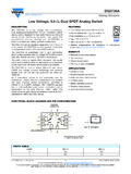
3 15 ns APPLICATIONS Test instrumentation Microwave radios and very small aperture terminals (VSATs) Military radios, radars, electronic counter measures (ECMs) Broadband telecommunications systems FUNCTIONAL BLOCK DIAGRAM RF2RF1 RFCENVSSCTRLVDD50 50 DRIVER14581-001 adrf5020 Figure 1. GENERAL DESCRIPTION The adrf5020 is a general-purpose, single-pole, double-throw (SPDT) Switch manufactured using a Silicon process. It comes in a 3 mm 3 mm, 20-terminal land grid array (LGA) package and provides high isolation and low insertion loss from 100 MHz to 30 GHz. This broadband Switch requires dual supply voltages, + V and V, and provides CMOS/LVTTL logic-compatible control.
4 adrf5020 data sheet Rev. B | Page 2 of 12 TABLE OF CONTENTS Features .. 1 Applications .. 1 Functional Block Diagram .. 1 General Description .. 1 Revision History .. 2 Specifications .. 3 Absolute Maximum Ratings .. 5 Power Derating Curves .. 5 ESD Caution .. 5 Pin Configuration and Function Descriptions .. 6 Interface 6 Typical Performance Characteristics ..7 Insertion Loss, Return Loss, and Isolation ..7 Input Power Compression and Third-Order Intercept (IP3) ..8 Theory of Operation ..9 Applications Information .. 10 Evaluation Board .. 10 Probe Matrix Board .. 11 Outline Dimensions.
5 12 Ordering Guide .. 12 REVISION HISTORY 4/2020 Rev. A to Rev. B Changes to Table 2 .. 5 Changes to Theory of Operation Section .. 9 2/2017 Rev. 0 to Rev. A Changed VEN = V to 5 V to VEN = 0 V or V to 5 V .. 3 7/2016 Revision 0: Initial Version data sheet adrf5020 Rev. B | Page 3 of 12 SPECIFICATIONS VDD = V to 5 V, VSS = V, VCTRL = 0 V or V to 5 V, VEN = 0 V or V to 5 V, TCASE = 25 C, 50 system, unless otherwise noted. Table 1. Parameter Symbol Test Conditions/Comments Min Typ Max Unit FREQUENCY RANGE 100 30,000 MHz INSERTION LOSS Between RFC and RF1/RF2 100 MHz to 10 GHz dB 10 GHz to 20 GHz dB 20 GHz to 30 GHz dB ISOLATION Between RFC and RF1/RF2 100 MHz to 10 GHz 65 dB 10 GHz to 20 GHz 60 dB 20 GHz to 30 GHz 60 dB Between RF1 and RF2 100 MHz to 10 GHz 70 dB 10 GHz to 20 GHz 65 dB 20 GHz to 30 GHz 65 dB RETURN LOSS RFC and RF1/RF2 (On) 100 MHz to 10 GHz 22 dB 10 GHz to 20 GHz 16 dB 20 GHz to 30 GHz 13 dB RF1/RF2 (Off )
6 100 MHz to 10 GHz 28 dB 10 GHz to 20 GHz 20 dB 20 GHz to 30 GHz 10 dB SWITCHING Rise and Fall Time tRISE, tFA L L 10% to 90% of RF output 2 ns On and Off Time tON, tOFF 50% VCTL to 90% of RF output 10 ns RF Settling Time dB 50% VCTL to dB of final RF output 15 ns dB 50% VCTL to dB of final RF output 20 ns INPUT LINEARITY1 600 MHz to 30 GHz Power Compression dB 26 dBm 1 dB P1dB 28 dBm Third-Order Intercept IP3 Two-tone input power = 14 dBm each tone, f = 1 MHz 52 dBm SUPPLY CURRENT VDD, VSS pins Positive IDD VDD = V 80 300 A VDD = 5 V 100 600 A Negative ISS VSS = V <1 10 A DIGITAL CONTROL INPUTS CTRL, EN pins Voltage Low VINL VDD = V 0 V VDD = 5 V V High VINH VDD = V V VDD = 5 V V Current Low and High IINL, IINH <1 A adrf5020 data sheet Rev.
7 B | Page 4 of 12 Parameter Symbol Test Conditions/Comments Min Typ Max Unit RECOMMENDED OPERATING CONDITONS Supply Voltage Positive VDD V Negative VSS V Digital Control Voltage VCTL 0 VDD V RF Input Power2 PIN f = 600 MHz to 30 GHz, TCASE = 85 C Through Path RF signal is applied to RFC or through connected RF1/RF2 24 dBm Terminated Path RF signal is applied to terminated RF1/RF2 24 dBm Hot Switching RF signal is present at RFC while switching between RF1 and RF2 18 dBm Case Temperature TCASE 40 +85 C 1 F or input linearity performance at frequencies less than 600 MHz, see Figure 15 to Figure 17.
8 2 F or power derating at frequencies less than 600 MHz, see Figure 2 t o Figure 4. data sheet adrf5020 Rev. B | Page 5 of 12 ABSOLUTE MAXIMUM RATINGS For recommended operating conditions, see Ta b l e 1. Table 2. Parameter Rating Supply Voltage Positive V to + V Negative V to + V Digital Control Inputs1 V to VDD + V or mA, whichever occurs first RF Input Power2 (f = 600 MHz to 30 GHz, TCASE) = 85 C) Through Path 27 dBm Terminated Path 25 dBm Hot Switching 21 dBm Temperature Junction (TJ) 135 C Storage 65 C to +150 C Reflow (MSL3 Rating)3 260 C Junction to Case Thermal Resistance ( JC) Through Path 420 C/W Terminated Path 160 C/W ESD Sensitivity HBM 1 kV (Class 1) 1 Overvoltages at digital control inputs are clamped by internal diodes.
9 The current must be limited to the maximum rating. 2 For power derating at frequencies less than 600 MHz, see Figure 2 to Figure 4. 3 See the Ordering Guide section. Stresses at or above those listed under Absolute Maximum Ratings may cause permanent damage to the product. This is a stress rating only; functional operation of the product at these or any other conditions above those indicated in the operational section of this specification is not implied. Operation beyond the maximum operating conditions for extended periods may affect product reliability. Only one absolute maximum rating can be applied at any one time.
10 POWER DERATING CURVES 4 14 12 10 8 6 4 202 POWER DERATING (dB)FREQUENCY (Hz)10k1M100M10G100k10M1G14581-002 Figure 2. Power Derating for Through Path vs. Frequency, TCASE = 85 C 4 14 12 10 8 6 4 202 POWER DERATING (dB)FREQUENCY (Hz)10k1M100M10G100k10M1G14581-003 Figure 3. Power Derating for Terminated Path vs. Frequency, TCASE = 85 C 4 14 12 10 8 6 4 202 POWER DERATING (dB)14581-004 FREQUENCY (Hz)10k1M100M10G100k10M1G Figure 4. Power Derating for Hot Switching vs. Frequency, TCASE = 85 C ESD CAUTION adrf5020 data sheet Rev. B | Page 6 of 12 PIN CONFIGURATION AND FUNCTION DESCRIPTIONS GNDRF2 GNDGNDGNDGNDGNDRF1 GNDGNDGNDGNDRFCGNDGNDGNDENVSSCTRLVDD1234 567891011121314151617181920 adrf5020 TOP VIEW(Not to Scale)NOTES1.