Transcription of 3-Channel Clock Generator, 24 Outputs Data Sheet AD9531
1 3-Channel Clock Generator, 24 OutputsData Sheet AD9531 Rev. 0 Document Feedback Information furnished by analog devices is believed to be accurate and reliable. However, no responsibility is assumed by analog devices for its use, nor for any infringements of patents or other rights of third parties that may result from its use. Specifications subject to change without notice. No license is granted by implication or otherwise under any patent or patent rights of analog devices . Trademarks and registered trademarks are the property of their respective owners. One Technology Way, Box 9106, Norwood, MA 02062-9106, : 2016 analog devices , Inc. All rights reserved. Technical Support FEATURES 3 fully integrated PLL/VCO cores (PLL1, PLL2, and PLL3) Jitter performance: ps rms typical PLL1, fractional-N mode, 12 kHz to 20 MHz bandwidth Loss of reference and lock detection for each PLL Pin-configurable common frequency translations Automatic synchronization of all Outputs on power-up Manual output synchronization capability Package available in an 88-lead LFCSP PLL1 details Fractional-N/integer-N modes Optional external VCXO Fixed delay mode for constant static phase offset 2 reference Clock inputs Input format: differential/single-ended Frequency range: MHz to 260 MHz Reference switching.
2 Manual/automatic 10 ultralow jitter HSTL/CMOS Outputs up to 400 MHz PLL2 details Integer-N mode (1 reference Clock input) Input format: differential/single-ended/crystal1 Frequency range: MHz to 250 MHz 12 HSTL/CMOS Outputs up to 400 MHz PLL3 details Integer-N mode (1 reference Clock input) Frequency range: MHz to 100 MHz Input format: differential/crystal (supports a 25 MHz to 50 MHz AT-cut quartz crystal resonator) 2 HSTL/LVDS/CMOS Outputs to 400 MHz/150 MHz (differential/CMOS) APPLICATIONS Radio equipment controller clocking Low jitter/phase noise Clock generation and distribution Clock generation and translation for SONET, 10GE, 10G FC, and other 10 Gbps protocols 40 Gbps/100 Gbps networking line cards, including SONET, synchronous ethernet, OTU2/3/4 Forward error correction ( ) High performance wireless transceivers ATE and high performance instrumentation Broadband infrastructures Ethernet line cards, switches, and routers SATA and PCI-express GENERAL DESCRIPTION The AD9531 provides a multioutput Clock generator function and three on-chip phase-locked loop (PLL)
3 Cores with SPI programmable output frequencies and formats. PLL1 provides two reference inputs and 10 Outputs and includes four user selectable loop configurations. The PLL has a fully integrated loop filter requiring only a single external capacitor (or a series RC network). PLL1 provides a wide range of output frequencies up to 400 MHz and is capable of operating with an external voltage controlled crystal oscillator (VCXO) and loop filter, instead of the integrated voltage controlled oscillator (VCO) and loop filter. PLL2 is an integer-N PLL providing a single reference input and 12 Outputs . PLL2 synthesizes output frequencies up to 400 MHz from the REF2_x source and synchronizes the output clocks to the input reference. PLL3 provides a single reference input and two Outputs .
4 PLL3 synthesizes output frequencies up to 400 MHz from the REF3_x source and synchronizes the output clocks to input reference. The AD9531 is available in an 88-lead LFCSP and is specified over the 40 C to +85 C operating temperature range. Throughout this data Sheet , multifunction pins, such as LOR/M4, are referred to either by the entire pin name or by a single function of the pin (for example, LOR, when only that function is relevant). In other cases, the text and figures of this data Sheet contain references to a channel rather than a pin. For example, REF_A refers to the REF_A channel rather than the REF_AP and REF_AN pins. Likewise, OUT3_1 refers to channel 1 of PLL3 rather than the OUT3_1P and OUT3_1N pins. Additionally, an abbreviated notation for a pin pair replaces an explicit reference to a each pin (for example, REF_Ax signifies the REF_AN and REF_AP pins.)
5 AD9531 data Sheet TABLE OF CONTENTS Features .. 1 Applications .. 1 General Description .. 1 Revision History .. 3 Functional Block Diagram .. 4 Specifications .. 5 Conditions .. 5 Supply Current .. 5 Power Dissipation .. 6 LDET1/M1, LDET2/M2, LDET3/M3, and LOR/M4 Pins .. 8 REF1_SEL Pin .. 8 PLL1 Characteristics .. 8 PLL2 Characteristics .. 13 PLL3 Characteristics .. 17 Serial Control Port .. 20 Absolute Maximum Ratings .. 21 ESD Caution .. 21 Pin Configuration and Function Descriptions .. 22 Typical Performance Characteristics .. 25 PLL1 Characteristics .. 25 PLL2 Characteristics .. 26 PLL3 Characteristics .. 27 General Characteristics .. 28 Terminology .. 29 Theory of Operation .. 30 PLL1 Integer/Fractional-N PLL .. 30 PLL1 Loop 31 PLL1 Reference Clock Inputs (REF1_Ax/REF1_Bx).
6 34 PLL1 Reference Frequency Scaling .. 34 PLL1 Phase Frequency Detector (PFD) and Charge Pumps .. 35 PLL1 Loop Filter .. 35 PLL1 Internal VCO .. 35 PLL1 VCO Divider (M1) .. 35 PLL1 External VCXO Input (RFIN1_x) .. 35 PLL1 Clock Distribution .. 36 PLL1 Holdover Mode and Freerun Mode .. 37 PLL1 Reference Selection Manual and Automatic .. 37 PLL1 Internal VCO Calibration .. 38 PLL1 - Modulator .. 40 PLL1 Lock Detector .. 40 PLL2 Integer-N PLL .. 41 PLL2 Reference Clock Input (REF2_P/REF2_N) .. 41 PLL2 Reference Divider (R2) .. 41 PLL2 PFD and Charge Pump .. 41 PLL2 Loop Filter .. 42 PLL2 VCO .. 42 PLL2 VCO Divider (M2) .. 44 PLL2 Feedback Divider (N2) .. 44 PLL2 Clock Distribution .. 44 PLL3 Integer-N PLL .. 46 PLL3 Reference Clock Input (REF3_P/REF3_N) .. 46 PLL3 Input Frequency Scaling.
7 46 PLL3 PFD and Charge Pumps .. 46 PLL3 Loop Filters .. 47 PLL3 VCOs .. 47 PLL3 Feedback Dividers .. 47 PLL3B Reference Divider (R3B) .. 47 PLL3 Clock Distribution .. 47 Additional Features .. 49 Power-On Reset (POR) .. 49 ROM Profiles .. 49 Multifunction Pins (LDET1/M1, LDET2/M2, LDET3/M3, LOR/M4) .. 49 Loss of Reference (LOR).. 50 PLL Lock Detection (LDETx) .. 51 Automatic output Synchronization .. 51 Serial Control Port .. 54 Serial Control Port Pin Descriptions .. 54 Operation of the Serial Control Port .. 54 Instruction Word (16 Bits) .. 55 MSB/LSB First Transfers .. 55 Register Map .. 57 Register Map Details .. 60 Serial Port Control Registers Register 0x0000 to Register 0x0005 .. 60 Device Identification and ROM Profile Registers Register 0x000A to Register 0x000E.
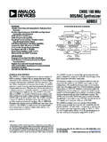
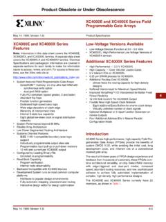
8 60 Status Registers Register 0x0080 to Register 0x0082 .. 61 LDET/LOR Control Registers Register 0x0083 to Register 0x0085 .. 61 PLL1 Registers .. 62 Rev. 0 | Page 2 of 88 data Sheet AD9531 Rev. 0 | Page 3 of 88 PLL2 Registers .. 69 PLL3 Registers .. 75 ROM Profile data .. 77 ROM Profile 0 to ROM Profile 15 .. 77 ROM Profile 16 to ROM Profile 31 .. 78 ROM Profile 32 to ROM PRofile 47 .. 80 ROM Profile 48 to ROM Profile 63 .. 82 Thermal Performance .. 84 Thermal Resistance .. 84 Applications Information .. 85 Interfacing to the Multifunction Pins .. 85 Interfacing to the RFIN1_x Pins .. 86 Driving REF2 or REF3 with V CMOS Logic .. 87 Using REF2 or REF3 with a Crystal Resonator .. 87 Outline Dimensions .. 88 Ordering Guide .. 88 REVISION HISTORY 1/16 Revision 0: Initial Version AD9531 data Sheet FUNCTIONAL BLOCK DIAGRAM PLL1 PLL2 D1A D1 CFRACTIONAL PLLINTEGRATED VCOINTEGER PLLINTEGRATEDVCOINTEGER PLLINTEGRATEDVCOSWITCHOVERCONTROL D3A3 LOCK DETECT PINS4 POWER-UP PROFILE SELECTSLOR (LOSS OF REFERENCE)PLL3 D1B4 OUTPUTSREF1_ALOR2 RFINAD9531 REF1_BREF1_SELREF2 SDIOREF3 SCLKCS4 OUTPUTS2 OUTPUTS2 OUTPUTS3 OUTPUTS3 OUTPUTS4 OUTPUTS1 OUTPUT1 OUTPUTLDET1/M1 LDET2/M2 LDET3/M3 LOR/M4 D3B D2A D2B D2C D2D3-WIRE SPIINTERFACE12973-001 Figure 1.
9 Rev. 0 | Page 4 of 88 data Sheet AD9531 SPECIFICATIONS Ty pi c a l values are given for V supplies at V 5% and V supplies at V 5%; TA = 25 C. Minimum and maximum values apply over the full variation of supply voltage and TA ( 40 C to +85 C) as listed in Ta b l e 1, unless otherwise specified. CONDITIONS Table 1. Parameter Min Typ Max Unit Test Conditions/Comments SUPPLY VOLTAGE 3 V Supply Pins V V 5% V Supply Pins V V 5% TEMPERATURE RANGE, TA 40 +25 +85 C SUPPLY CURRENT Table 2. Parameter Min Typ Max Unit Test Conditions/Comments SUPPLY CURRENT Case 1 PLL1: off; PLL2: off; PLL3: off V Supply PLL1 Pins 6 mA PLL2 Pins 19 mA PLL3 Pins mA DVDD 3 mA V Supply PLL1 Pins mA PLL2 Pins mA PLL3 Pins mA Case 2 PLL1: differential input at MHz, HSTL output at MHz, all Outputs active, internal VCO; PLL2: off; PLL3: off V Supply PLL1 Pins 270 mA PLL2 Pins 19 mA PLL3 Pins mA DVDD mA V Supply PLL1 Pins 34 mA PLL2 Pins mA PLL3 Pins mA Case 3 PLL1: off; PLL2: V, CMOS input at 50 MHz, HSTL output at MHz, all Outputs active.
10 PLL3: off V Supply PLL1 Pins 6 mA PLL2 Pins 280 mA PLL3 Pins mA DVDD Pin mA V Supply PLL1 Pins mA PLL2 Pins 22 mA PLL3 Pins mA Rev. 0 | Page 5 of 88 AD9531 data Sheet Parameter Min Typ Max Unit Test Conditions/Comments Case 4 PLL1: off; PLL3: V, CMOS input at 25 MHz, OUT3_0 and OUT3_1 at 125 MHz ( V CMOS and HSTL, respectively); PLL2: off V Supply PLL1 Pins 6 mA PLL2 Pins 19 mA PLL3 Pins 72 mA DVDD Pin mA V Supply PLL1 Pins mA PLL2 Pins mA PLL3 Pins mA Case 5 PLL1: differential input at MHz, HSTL output at MHz, all Outputs active, internal VCO; PLL2: V, CMOS input at 50 MHz, HSTL output at MHz, all Outputs active; PLL3: V, CMOS input at 25 MHz, OUT3_0 and OUT3_1 at 125 MHz ( V CMOS and HSTL, respectively) V Supply PLL1 Pins 270 mA PLL2 Pins 280 mA PLL3 Pins 72 mA DVDD Pin mA V Supply PLL1 Pins 34 mA PLL2 Pins 23 mA PLL3 Pins mA INCREMENTAL SUPPLY CURRENT PLL1, External VCXO Configuration V Supply (PLL1 Pins) 22 mA V Supply (PLL1 Pins) 27 mA PLL3, Dual Loop Configuration V Supply (PLL3 Pins) 36 mA V Supply (PLL3 Pins) 0 mA POWER DISSIPATION Table 3.