Transcription of AD9851 CMOS 180 MHz DDS/DAC Synthesizer Data Sheet …
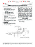
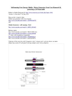
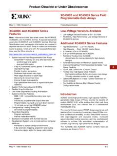
1 CMOS 180 MHz DDS/DAC Synthesizer AD9851 . FEATURES FUNCTIONAL BLOCK DIAGRAM. 180 MHz clock Rate with Selectable 6 Reference clock Multiplier +VS GND. On-Chip High Performance 10-Bit DAC and High Speed AD9851 . Comparator with Hysteresis DAC RSET. SFDR >43 dB @ 70 MHz AOUT REF. clock IN. 6 REFCLK. MULTIPLIER 10-BIT. HIGH SPEED ANALOG. 32-Bit Frequency Tuning Word MASTER DDS DAC OUT. Simplified Control Interface: Parallel or Serial RESET. PHASE. Asynchronous Loading Format 32-BIT AND. TUNING CONTROL ANALOG. 5-Bit Phase Modulation and Offset Capability WORD WORDS IN. FREQUENCY. Comparator Jitter <80 ps p-p @ 20 MHz UPDATE/DATA FREQUENCY/PHASE. REGISTER DATA REGISTER. V to V Single-Supply Operation RESET. clock OUT. Low Power: 555 mW @ 180 MHz WORD LOAD DATA INPUT REGISTER clock OUT. clock . Power-Down Function, 4 mW @ V SERIAL PARALLEL COMPARATOR. LOAD. Ultrasmall 28-Lead SSOP Packaging LOAD.
2 1 BIT 8 BITS . APPLICATIONS 40 LOADS 5 LOADS. Frequency/Phase-Agile Sine Wave Synthesis FREQUENCY, PHASE. AND CONTROL DATA INPUT. clock Recovery and Locking Circuitry for Digital Communications Digitally Controlled ADC Encode Generator Agile Local Oscillator Applications in Communications Quadrature Oscillator CW, AM, FM, FSK, MSK Mode Transmitter GENERAL DESCRIPTION The AD9851 contains an internal high speed comparator that The AD9851 is a highly integrated device that uses advanced can be configured to accept the (externally) filtered output of the DDS technology, coupled with an internal high speed, high DAC to generate a low jitter output pulse. performance D/A converter, and comparator, to form a digitally The frequency tuning, control, and phase modulation words are programmable frequency Synthesizer and clock generator func- asynchronously loaded into the AD9851 via a parallel or serial tion.
3 When referenced to an accurate clock source, the AD9851 loading format. The parallel load format consists of five iterative generates a stable frequency and phase-programmable digitized loads of an 8-bit control word (byte). The first 8-bit byte controls analog output sine wave. This sine wave can be used directly as output phase, 6 REFCLK Multiplier, power-down enable and a frequency source, or internally converted to a square wave for loading format; the remaining bytes comprise the 32-bit frequency agile- clock generator applications. The AD9851 's innovative tuning word. Serial loading is accomplished via a 40-bit serial data high speed DDS core accepts a 32-bit frequency tuning word, stream entering through one of the parallel input bus lines. The which results in an output tuning resolution of approximately AD9851 uses advanced CMOS technology to provide this break- Hz with a 180 MHz system clock .
4 The AD9851 contains through level of functionality on just 555 mW of power dissipation a unique 6 REFCLK Multiplier circuit that eliminates the (5 V supply), at the maximum clock rate of 180 MHz. need for a high speed reference oscillator. The 6 REFCLK. Multiplier has minimal impact on SFDR and phase noise char- The AD9851 is available in a space-saving 28-lead SSOP, acteristics. The AD9851 provides five bits of programmable surface-mount package that is pin-for-pin compatible with the phase modulation resolution to enable phase shifting of its popular AD9850 125 MHz DDS. It is specified to operate over output in increments of . the extended industrial temperature range of 40 C to +85 C. at > V supply voltage. Below V, the specifications apply over the commercial temperature range of 0 C to 85 C. REV. D. Information furnished by Analog Devices is believed to be accurate and reliable.
5 However, no responsibility is assumed by Analog Devices for its use, nor for any infringements of patents or other rights of third parties that may result from its use. No license is granted by implication or oth- One Technology Way, Box 9106, Norwood, MA 02062-9106, erwise under any patent or patent rights of Analog Devices. Trademarks Tel: 781/329-4700 and registered trademarks are the property of their respective owners. Fax: 781/326-8703 2004 Analog Devices, Inc. All rights reserved. AD9851 SPECIFICATIONS (VS1 = 5 V 5%, RSET = k , 6 REFCLK Multiplier Disabled, External Reference clock = 180 MHz, except as noted.). Test AD9851 BRS. Parameter Temp Level Min Typ Max Unit clock INPUT CHARACTERISTICS. Frequency Range (6 REFCLK Multiplier Disabled). V Supply Full IV 1 180 MHz V Supply Full IV 1 125 MHz V Supply 0 C to 85 C IV 1 100 MHz Frequency Range (6 REFCLK Multiplier Enabled).
6 V Supply Full IV 5 30 MHz V Supply Full IV 5 MHz V Supply 0 C to 85 C IV 5 MHz Duty Cycle Full IV 45 60 %. Duty Cycle (6 REFCLK Multiplier Enabled) Full IV 35 65 %. Input Resistance 25 C V 1 M . Minimum Switching Thresholds2. Logic 1, V Supply 25 C IV V. Logic 1, V Supply 25 C IV V. Logic 0, V Supply 25 C IV V. Logic 0, V Supply 25 C IV 1 V. DAC OUTPUT CHARACTERISTICS. Full-Scale Output Current 25 C IV 5 10 20 mA. Gain Error 25 C I 10 +10 % FS. Output Offset 25 C I 10 A. Differential Nonlinearity 25 C I LSB. Integral Nonlinearity 25 C I 1 LSB. Residual Phase Noise, MHz, 1 kHz Offset PLL On 25 C V 125 dBc/Hz PLL Off 25 C V 132 dBc/Hz Output Impedance 25 C V 120 k . Voltage Compliance Range 25 C I + V. Wideband Spurious-Free Dynamic Range MHz Analog Out (DC to 72 MHz) 25 C IV 60 64 dBc MHz Analog Out (DC to 72 MHz) 25 C IV 51 53 dBc MHz Analog Out (DC to 72 MHz) 25 C IV 51 55 dBc MHz Analog Out (DC to 72 MHz) 25 C IV 46 53 dBc MHz Analog Out (DC to 72 MHz) 25 C IV 42 43 dBc Narrowband Spurious-Free Dynamic Range MHz ( 50 kHz) 25 C V 85 dBc MHz ( 200 kHz) 25 C V 80 dBc MHz ( 50 kHz) 25 C V 85 dBc MHz ( 200 kHz) 25 C V 80 dBc MHz ( 50 kHz) 25 C V 85 dBc MHz ( 200 kHz) 25 C V 73 dBc COMPARATOR INPUT CHARACTERISTICS.
7 Input Capacitance 25 C V 3 pF. Input Resistance 25 C IV 500 k . Input Bias Current 25 C I 12 A. Input Voltage Range 25 C IV 0 5 V. COMPARATOR OUTPUT CHARACTERISTICS. Logic 1 Voltage 5 V Supply 25 C VI V. Logic 1 Voltage V Supply 25 C VI V. Logic 1 Voltage V Supply 25 C VI V. Logic 0 Voltage 25 C VI + V. Continuous Output Current 25 C IV 20 mA. Hysteresis 25 C IV 10 mV. Propagation Delay 25 C IV 7 ns Toggle Frequency (1 V p-p Input Sine Wave) 25 C IV 200 MHz Rise/Fall Time, 15 pF Output Load 25 C IV 7 ns Output Jitter (p-p)3 25 C IV 80 ps (p-p). clock OUTPUT CHARACTERISTICS. Output Jitter ( clock Generator Configuration, 40 MHz 1 V p-p Input Sine Wave) 25 C V 250 ps (p-p). clock Output Duty Cycle Full IV 50 10 %. 2 REV. D. AD9851 . Test AD9851 BRS. Parameter Temp Level Min Typ Max Unit 4. TIMING CHARACTERISTICS. tWH, tWL (W_CLK Min Pulse Width High/Low) Full IV ns tDS, tDH (Data to W_CLK Setup and Hold Times) Full IV ns tFH, tFL (FQ_UD Min Pulse Width High/Low) Full IV 7 ns tCD (REFCLK Delay After FQ_UD)5 Full IV ns tFD (FQ_UD Min Delay After W_CLK) Full IV 7 ns tCF (Output Latency from FQ_UD).
8 Frequency Change Full IV 18 SYSCLK. Cycles Phase Change Full IV 13 SYSCLK. Cycles tRH (CLKIN Delay After RESET Rising Edge) Full IV ns tRL (RESET Falling Edge After CLKIN) Full IV ns tRR (Recovery from RESET) Full IV 2 SYSCLK. Cycles tRS (Minimum RESET Width) Full IV 5 SYSCLK. Cycles tOL (RESET Output Latency) Full IV 13 SYSCLK. Cycles Wake-Up Time from Power-Down Mode6 25 C V 5 s CMOS LOGIC INPUTS. Logic 1 Voltage, 5 V Supply 25 C I V. Logic 1 Voltage, V Supply 25 C IV V. Logic 1 Voltage, V Supply 25 C IV V. Logic 0 Voltage 25 C IV V. Logic 1 Current 25 C I 12 A. Logic 0 Current 25 C I 12 A. Rise/Fall Time 25 C IV 100 ns Input Capacitance 25 C V 3 pF. POWER SUPPLY. VS6 Current @: MHz clock , V Supply 25 C VI 30 35 mA. 100 MHz clock , V Supply 25 C VI 40 50 mA. MHz clock , V Supply 25 C VI 35 45 mA. 125 MHz clock , V Supply 25 C VI 55 70 mA. MHz clock , 5 V Supply 25 C VI 50 65 mA. 125 MHz clock , 5 V Supply 25 C VI 70 90 mA.
9 180 MHz clock , 5 V Supply 25 C VI 110 130 mA. Power Dissipation @ : MHz clock , 5 V Supply 25 C VI 250 325 mW. MHz clock , V Supply 25 C VI 115 150 mW. MHz clock , V Supply 25 C VI 85 95 mW. 100 MHz clock , V Supply 25 C VI 110 135 mW. 125 MHz clock , 5 V Supply 25 C VI 365 450 mW. 125 MHz clock , V Supply 25 C VI 180 230 mW. 180 MHz clock , 5 V Supply 25 C VI 555 650 mW. PDISS Power-Down Mode @: 5 V Supply 25 C VI 17 55 mW. V Supply 25 C VI 4 20 mW. NOTES. 1. +VS collectively refers to the positive voltages applied to DVDD, PVCC, and AVDD. Voltages applied to these pins should be of the same potential. 2. Indicates the minimum signal levels required to reliably clock the device at the indicated supply voltages. This specifies the p-p signal level and dc offset needed when the clocking signal is not of CMOS/TTL origin, , a sine wave with 0 V dc offset. 3. The comparator's jitter contribution to any input signal.
10 This is the minimum jitter on the outputs that can be expected from an ideal input. Considerably more output jitter is seen when nonideal input signals are presented to the comparator inputs. Nonideal characteristics include the presence of extraneous, nonharmonic signals (spur's, noise), slower slew rate, and low comparator overdrive. 4. Timing of input signals FQ_UD, WCLK, RESET are asynchronous to the reference clock ; however, the presence of a reference clock is required to implement those functions. In the absence of a reference clock , the AD9851 automatically enters power-down mode rendering the IC, including the comparator, inoperable until a refer- ence clock is restored. Very high speed updates of frequency/phase word will require FQ_UD and WCLK to be externally synchronized with the external reference clock to ensure proper timing. 5. Not applicable when 6 REFCLK Multiplier is engaged.