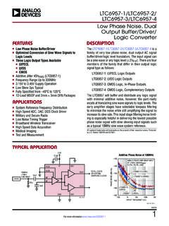
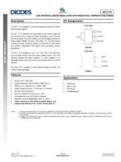
Transcription of 74HC86 Description Pin Assignments
1 74HC86 Document number: DS35325 Rev. 3 - 2 1 of 9 January 2013 Diodes Incorporated 74HC86 QUADRUPLE 2- input EXCULSIVE OR GATES Description The 74HC86 provides provides four independent 2- input Exclusive OR gates with standard push-pull outputs. The device is designed for operation with a power supply range of to The gates perform the Boolean function: BAY = or BABAY+= Features Wide Supply Voltage Range from to Sinks or sources 4mA at VCC = CMOS low power consumption Schmitt Trigger Action at All Inputs ESD Protection Exceeds JESD 22 200-V Machine Model (A115-A) 2000-V Human Body Model (A114-A) Exceeds 1000-V Charged Device Model (C101C) Range of Package Options SO-14 and TSSOP-14 Totally Lead-Free & Fully RoHS Compliant (Notes 1 & 2) Halogen and Antimony Free.
2 Green Device (Note 3) Pin Assignments Applications General Purpose Logic Wide array of products such as: PCs, Networking, Notebooks, Netbooks Computer Peripherals, Hard Drives, CD/DVD ROM TV, DVD, DVR, Set Top Box Notes: 1. No purposely added lead. Fully EU Directive 2002/95/EC (RoHS) & 2011/65/EU (RoHS 2) compliant. 2. See for more information about Diodes Incorporated s definitions of Halogen- and Antimony-free, "Green" and Lead-free. 3. Halogen- and Antimony-free "Green products are defined as those which contain <900ppm bromine, <900ppm chlorine (<1500ppm total Br + Cl) and <1000ppm antimony compounds. 74HC86 Document number: DS35325 Rev. 3 - 2 2 of 9 January 2013 Diodes Incorporated 74HC86 Pin descriptions Pin Number Pin Name Function 1 1A Data input 2 1B Data input 3 1Y Data Output 4 2A Data input 5 2B Data input 6 2Y Data
3 Output 7 GND Ground 8 3Y Data Output 9 3A Data input 10 3B Data input 11 4Y Data Output 12 4A Data input 13 4B Data input 14 VCC Supply Voltage Logic Diagram Function Table Inputs Output A B Y L L L L H H H L H H H L 74HC86 Document number: DS35325 Rev.
4 3 - 2 3 of 9 January 2013 Diodes Incorporated 74HC86 Absolute Maximum Ratings (Note 4) (@TA = +25 C, unless otherwise specified.) Symbol Description Rating Unit ESD HBM Human Body Model ESD Protection 2 KV ESD CDM Charged Device Model ESD Protection 1 KV ESD MM Machine Model ESD Protection 200 V VCC Supply Voltage Range to + V VI input Voltage Range (Note 5) to + V IIK input Clamp Current VI < or Vi > VCC + 20 mA IOK Output Clamp Current VO < or VO > VCC + 20 mA IO Continuous output current < VO VCC + +/- 25 mA ICC Continuous Current Through Vcc 50 mA IGND Continuous Current Through GND -50 mA TJ Operating Junction Temperature -40 to +150 C TSTG Storage Temperature -65 to +150 C PTOT Total Power Dissipation 500 mW Notes: 4.
5 Stresses beyond the absolute maximum may result in immediate failure or reduced reliability. These are stress values and device operation should be within recommend values. 5. input Voltage cannot exceed VCC to the extent the Maximum clamp current is exceeded. Recommended Operating Conditions (Note 6) (@TA = +25 C, unless otherwise specified.) Symbol Parameter Conditions Min Max Unit VCC Supply Voltage V VI input Voltage 0 VCC V VO Output Voltage 0 VCC V t/ V input Transition Rise or Fall Rate VCC = 625 ns/V VCC = 140 VCC = 85 TA Operating Free-Air Temperature -40 +125 C
6 Note: 6. Unused inputs should be held at VCC or Ground. 74HC86 Document number: DS35325 Rev. 3 - 2 4 of 9 January 2013 Diodes Incorporated 74HC86 Electrical Characteristics (@TA = +25 C, unless otherwise specified.) Symbol Parameter Test Conditions VCC TA = -40 C to +85 C TA = -40 C to +125 C Unit Min Max Min Max VIH High-level input Voltage V VIL Low-level input voltage V
7 VOH High-level Output Voltage IOH = -20 A V IOH = -20 A IOH = -20 A IOH = IOH = VOL Low-level Output Voltage IOL = 20 A V IOL = 20 A IOL = 20 A IOL = 4mA IOL = II input Current VI =GND to 1 1 A ICC Supply Current VI = GND or VCC.
8 IO = 0 20 40 A Switching Characteristics Symbol Parameter Test Conditions VCC TA = +25 C -40 C to +85 C -40 C to +125 C Unit Min Typ. Max Max Max tPD Propagation Delay AN to YN Figure 1 CL = 50pF 25 90 115 135 ns 9 18 23 27 7 15 20 23 tt Transition time Figure 1 CL = 50pF 19 75 95 110 ns 7 15 19 22 6 13 16 19 Operating Characteristics (@TA = +25 C, unless otherwise specified.)
9 Parameter Test Conditions VCC = 6V Unit Typ Cpd Power Dissipation Capacitance per Gate f = 1 MHz 25 pF CI input Capacitance VI = VCC or GND 4 pF 74HC86 Document number: DS35325 Rev. 3 - 2 5 of 9 January 2013 Diodes Incorporated 74HC86 Parameter Measurement Information VCC Inputs VM CL VI tr/tf to VCC 6ns VCC/2 15pF, 50pF Voltage Waveform Pulse Duration Voltage Waveform Propagation Delay Times Inverting and Non Inverting Outputs Notes: A. Includes test lead and test apparatus capacitance. B. All pulses are supplied at pulse repetition rate 1 MHz.
10 C. Inputs are measured separately one transition per measurement. D. tPLH and tPHL are the same as tPD. Figure 1 Load Circuit and Voltage Waveforms 74HC86 Document number: DS35325 Rev. 3 - 2 6 of 9 January 2013 Diodes Incorporated 74HC86 Ordering Information Device Package Code Packaging 7 Tape and Reel Quantity Part Number Suffix 74HC86S14-13 S14 SO-14 2500/Tape & Reel -13 74HC86T14-13 T14 TSSOP-14 2500/Tape & Reel -13 Marking Information (1) SO-14, TSSOP-14 Part Number Package 74HC86S14 SO-14 74HC86T14 TSSOP-14 74HC86 Document number: DS35325 Rev. 3 - 2 7 of 9 January 2013 Diodes Incorporated 74HC86 Package Outline Dimensions (All dimensions in mm.)