Example: tourism industry
LF353-NWide Bandwidth Dual JFET Input Operational Amplifier
1FEATURES DESCRIPTION These devices are low cost, high speed, dual JFET 2• Internally Trimmed Offset Voltage: 10 mV input operational amplifiers with an internally trimmed • Low Input Bias Current: 50pA input offset voltage (BI-FET II technology). They • Low Input Noise Voltage: 25 nV/√Hz require low supply current yet maintain a large gain
Tags:
Information
Domain:
Source:
Link to this page:
Documents from same domain

LMC6482 CMOS Dual Rail-To-Rail Input and Output ...
www.ti.comLMC6482 www.ti.com SNOS674E –NOVEMBER 1997–REVISED APRIL 2015 5 Pin Configuration and Functions D, DGK and P Packages 8-Pin SOIC, VSSOP and PDIP (Top View) Pin Functions PIN TYPE DESCRIPTION NO.

LM136-2.5,LM236-2.5,LM336-2 - TI.com
www.ti.comLM136-2.5/LM236-2.5/LM336-2.5V Reference Diode General Description The LM136-2.5/LM236-2.5 and LM336-2.5 integrated cir-cuits are …

SimpleLink™ CC3120, CC3220 Wi-Fi ... - Texas …
www.ti.comUser User x x x x x x x x x x x x x x x x x x x x Application Servers Vendor IoT Devices Internet Introduction www.ti.com 4 SWRA509A–February 2017–Revised March 2017 Submit Documentation Feedback

www.ti.com SNVS749F - Texas Instruments
www.ti.comLM136-2.5-N SNVS749F – MAY 1998– REVISED APRIL 2013 www.ti.com Typical Performance Characteristics (continued) Temperature Drift Figure 13. …

MSP430x2xx Family User's Guide (Rev. J) - TI.com
www.ti.comMSP430x2xx Family User's Guide Literature Number: SLAU144J December 2004– Revised July 2013

1.8-V Micropower CMOS Operational Amplifier …
www.ti.com5 OPA2333-HT www.ti.com SBOS483I –JULY 2009–REVISED MAY 2015 Product Folder Links: OPA2333-HT Copyright © 2009–2015, Texas Instruments Incorporated Submit Documentation Feedback

OPAx354 250-MHz, Rail-to-Rail I/O, CMOS …
www.ti.comOPA354 IN +IN V OUT V+ V Product Folder Order Now Technical Documents Tools & Software Support & Community Reference Design An IMPORTANT NOTICE at the end of this data sheet addresses availability, warranty, changes, use …

Analog linearization of resistance temperature …
www.ti.com21 Analog Applications Journal Texas Instruments Incorporated 4Q 2011 www.ti.com/aaj High-Performance Analog Products …

TMS320C28x DSP/BIOS 5.x Application …
www.ti.comSPRU625L—August 2012 API Functional Overview 9 Submit Documentation Feedback www.ti.com Naming Conventions 1.2 Naming Conventions The format for a DSP/BIOS operation name is a 3- or 4-letter prefix for the module that contains the

WL18x7MOD WiLink™ 8 Dual-Band Industrial …
www.ti.comProduct Folder Order Now Technical Documents Tools & Software Support & Community Reference Design An IMPORTANT NOTICE at the end of this data sheet addresses availability, warranty, changes, use in safety-critical applications,
Related documents
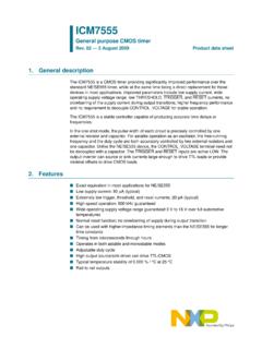
ICM7555 General purpose CMOS timer
www.nxp.com2 3 4 6 5 8 7 Table 2. Pin description Symbol Pin Description GND 1 supply ground TRIGGER 2 start timer input; (active LOW) OUTPUT 3 timer logic level output RESET 4 timer inhibit input; (active LOW) CONTROL_VOLTAGE 5 timing capacitor upper voltage sense input THRESHOLD 6 timing capacitor lower voltage sense input DISCHARGE 7 timing capacitor ...
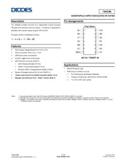
74HC86 Description Pin Assignments
www.diodes.comQUADRUPLE 2-INPUT EXCULSIVE OR GATES Description The 74HC86 provides provides four independent 2-input Exclusive OR gates with standard push-pull outputs. The device is designed for operation with a power supply range of 2.0V to 6.0V. The gates perform the Boolean function: Y =A ...
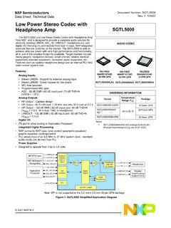
SGTL5000, Low Power Stereo Codec with Headphone Amp - …
www.nxp.comA functional description can be found in Functional Description, beginning on page 12. Table 1. SGTL5000 Pin Definitions 20 Pin QFN 32 Pin QFN Pin Name Pin Function Formal Name Definition 1 2 HP_R Analog Right headphone output ... MIC Input Impedance - 2.9 - k ...

Job description Senior Employee Engagement ...
www.intoglobal.comJob description Senior Employee Engagement & Communications Manager November 2019. Page 2 of 4 ... o Provide input on the design of the employee surveys and support the internal communications efforts in communicating the results to key stakeholders in a timely fashion.
Mathematical description of EM waves
pages.mtu.edu2/3/14 15 The Forced Oscillator: The relative phase of the oscillator motion with respect to the input force depends on the frequencies. Below resonance ω << ω 0 Force Oscillator On resonance ω = ω 0 Above resonance ω >> ω 0 Let the oscillator’s resonant frequency be ω 0, and the forcing frequency be ω. We could think of the
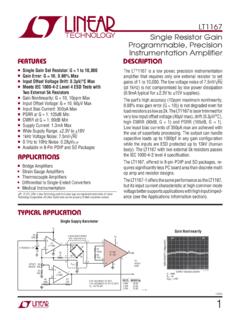
LT1167 - Single Resistor Gain Programmable, Precision ...
www.analog.comin Input Noise Current fO = 0.1Hz to 10Hz 10 10 pAP-P Input Noise Current Densty fO = 10Hz 124 124 fA/√Hz RIN Input Resistance VIN CIN(DIFF) Differential Input Capacitance fO = 100kHz 1.6 1.6 pF CIN(CM) Common Mode Input Capacitance fO = 100kHz 1.6 1.6 pF VCM Input Voltage Range G = 1, Other Input Grounded VS = ±2.3V to ±5V VS = ±5V to ± ...
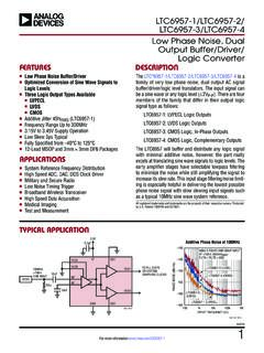
LTC6957-1/LTC6957-2/LTC6957-3/LTC6957-4 - Low Phase …
www.analog.comVINSE Input Signal Level Range, Single-Ended l 0.2 0.8 2 VP-P VINDIFF Input Signal Level Range, Differential l 0.2 0.8 2 VP-P tMIN Minimum Input Pulse Width High or Low 0.5 ns VINCM Self-Bias Voltage, IN+, IN– l 1.8 2 2.3 V RIN Input Resistance, Differential l 1.5 2 2.5 kΩ CIN Input Capacitance, Differential 0.5 pF BWIN ++ + LTC6957-2
The Variant Call Format (VCF) Version 4.2 Specification
samtools.github.io1.2.3 Filter field format FILTERs that have been applied to the data should be described as follows: ##FILTER=<ID=ID,Description="description"> 1.2.4 Individual format field format Likewise, Genotype fields specified in the FORMAT field should be described as follows: ##FORMAT=<ID=ID,Number=number,Type=type,Description="description">
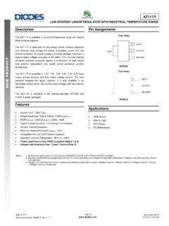
3 INPUT - Diodes Incorporated
www.diodes.comINPUT OUTPUT GND 10PF 22PF 3.3V V OUT =V REF * ( 1+R2/R1) + I ADJ * R2 3 1 2 2 1 3 Note 4: The AZ1117I is compatible with low ESR ceramic capacitor. The ESR of the output capacitors must be less than 20Ω. A minimum of 10µF output capacitor is required. Functional Block Diagram 2 Thermal Protection +-For Adjustable Output, disconnect A1 and A2 ...