Transcription of 8-bit Atmel Microcontroller with 128KBytes
1 Features High-performance, Low-power Atmel AVR 8-bit Microcontroller Advanced RISC Architecture 133 Powerful Instructions Most Single Clock Cycle Execution 32 x 8 General Purpose Working Registers + Peripheral Control Registers Fully Static Operation Up to 16 MIPS Throughput at 16 MHz On-chip 2-cycle Multiplier High Endurance Non-volatile Memory segments 128 Kbytes of In-System Self-programmable Flash program memory 4 Kbytes EEPROM 4 Kbytes Internal SRAM Write/Erase cycles: 10,000 Flash/100,000 EEPROM Data retention: 20 years at 85 C/100 years at 25 C(1) Optional Boot Code Section with Independent Lock BitsIn-System Programming by On-chip Boot ProgramTrue Read-While-Write Operation Up to 64 Kbytes Optional External Memory Space Programming Lock for Software Security SPI Interface for In-System Programming QTouch library support Capacitive touch buttons, sliders and wheels QTouch and QMatrix acquisition Up to 64 sense channels JTAG (IEEE std.)
2 Compliant) Interface Boundary-scan Capabilities According to the JTAG Standard Extensive On-chip Debug Support Programming of Flash, EEPROM, Fuses and Lock Bits through the JTAG Interface Peripheral Features Two 8-bit Timer/Counters with Separate Prescalers and Compare Modes Two Expanded 16-bit Timer/Counters with Separate Prescaler, Compare Mode and Capture Mode Real Time Counter with Separate Oscillator Two 8-bit PWM Channels 6 PWM Channels with Programmable Resolution from 2 to 16 Bits Output Compare Modulator 8-channel.
3 10-bit ADC8 Single-ended Channels7 Differential Channels2 Differential Channels with Programmable Gain at 1x, 10x, or 200x Byte-oriented Two-wire Serial Interface Dual Programmable Serial USARTs Master/Slave SPI Serial Interface Programmable Watchdog Timer with On-chip Oscillator On-chip Analog Comparator Special Microcontroller Features Power-on Reset and Programmable Brown-out Detection Internal Calibrated RC Oscillator External and Internal Interrupt Sources Six Sleep Modes: Idle, ADC Noise Reduction, Power-save, Power-down, Standby, and Extended Standby Software Selectable Clock Frequency ATmega103 Compatibility Mode Selected by a Fuse Global Pull-up Disable I/O and Packages 53 Programmable I/O Lines 64-lead TQFP and 64-pad QFN/MLF Operating Voltages - ATmega128L - ATmega128 Speed Grades 0 - 8 MHz ATmega128L 0 - 16 MHz ATmega1288-bit Atmel Microcontroller with 128 KBytes In-SystemProgrammable FlashATmega128 ATmega128 LSummaryRev.
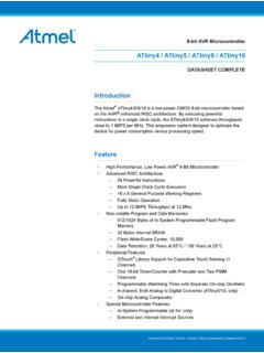
4 2467XS AVR 06/1122467XS AVR 06/11 ATmega128 Pin ConfigurationsFigure 1. Pinout ATmega128 Note:The Pinout figure applies to both TQFP and MLF packages. The bottom pad under the QFN/MLFpackage should be soldered to Atmel AVR ATmega128 is a low-power CMOS 8-bit Microcontroller based on the AVRenhanced RISC architecture. By executing powerful instructions in a single clock cycle, theATmega128 achieves throughputs approaching 1 MIPS per MHz allowing the system designer tooptimize power consumption versus processing (PDI) PE0(TXD0/PDO) PE1(XCK0/AIN0) PE2(OC3A/AIN1) PE3(OC3B/INT4) PE4 (OC3C/INT5) PE5(T3/INT6) PE6(ICP3/INT7) PE7(SS) PB0(SCK) PB1(MOSI) PB2(MISO) PB3(OC0) PB4(OC1A) PB5(OC1B) PB6PA3 (AD3)PA4 (AD4)PA5 (AD5)PA6 (AD6)PA7 (AD7)PG2(ALE)PC7 (A15)PC6 (A14)PC5 (A13)PC4 (A12)PC3 (A11) PC2 (A10)PC1 (A9)PC0 (A8) PG1(RD)PG0(WR)
5 6463626160595857565554535251504917181920 212223242526272829303132 (OC2/OC1C) PB7 TOSC2/PG3 TOSC1/PG4 RESETVCCGNDXTAL2 XTAL1 (SCL/INT0) PD0 (SDA/INT1) PD1 (RXD1/INT2) PD2 (TXD1/INT3) PD3 (ICP1) PD4(XCK1) PD5 (T1) PD6 (T2) PD7 AVCCGNDAREFPF0 (ADC0)PF1 (ADC1)PF2 (ADC2)PF3 (ADC3)PF4 (ADC4/TCK)PF5 (ADC5/TMS) PF6 (ADC6/TDO)PF7 (ADC7/TDI)GNDVCCPA0 (AD0) PA1 (AD1)PA2 (AD2)32467XS AVR 06/11 ATmega128 Block DiagramFigure 2. Block DiagramPROGRAMCOUNTERINTERNALOSCILLATORW ATCHDOGTIMERSTACKPOINTERPROGRAMFLASHMCU CONTROLREGISTERSRAMGENERALPURPOSEREGISTE RSINSTRUCTIONREGISTERTIMER/COUNTERSINSTR UCTIONDECODERDATA PORTBDATA PORTEDATA PORTADATA PORTDDATA REGISTERPORTBDATA REGISTERPORTEDATA REGISTERPORTADATA REGISTERPORTDTIMING ANDCONTROLOSCILLATOROSCILLATORINTERRUPTU NITEEPROMSPIUSART0 STATUSREGISTERZYXALUPORTB DRIVERSPORTE DRIVERSPORTA DRIVERSPORTF DRIVERSPORTD DRIVERSPORTC DRIVERSPB0 - PB7PE0 - PE7PA0 - PA7PF0 - PF7 RESETVCCAGNDGNDAREFXTAL1 XTAL2
6 CONTROLLINES+-ANALOGCOMPARATORPC0 - PC78-BIT DATA BUSAVCCUSART1 CALIB. OSCDATA PORTCDATA REGISTERPORTCON-CHIP DEBUGJTAG TAPPROGRAMMINGLOGICPENBOUNDARY- SCANDATA PORTFDATA REGISTERPORTFADCPD0 - PD7 DATA PORTGDATA DRIVERSPG0 - PG4 TWO-WIRE SERIALINTERFACE42467XS AVR 06/11 ATmega128 The Atmel AVR core combines a rich instruction set with 32 general purpose working regis-ters. All the 32 registers are directly connected to the Arithmetic Logic Unit (ALU), allowing twoindependent registers to be accessed in one single instruction executed in one clock cycle.
7 Theresulting architecture is more code efficient while achieving throughputs up to ten times fasterthan conventional CISC ATmega128 provides the following features: 128 Kbytes of In-System Programmable Flashwith Read-While-Write capabilities, 4 Kbytes EEPROM, 4 Kbytes SRAM, 53 general purpose I/Olines, 32 general purpose working registers, Real Time Counter (RTC), four flexible Timer/Coun-ters with compare modes and PWM, 2 USARTs, a byte oriented Two-wire Serial Interface, an 8-channel, 10-bit ADC with optional differential input stage with programmable gain, programma-ble Watchdog Timer with Internal Oscillator, an SPI serial port, IEEE std.
8 CompliantJTAG test interface, also used for accessing the On-chip Debug system and programming andsix software selectable power saving modes. The Idle mode stops the CPU while allowing theSRAM, Timer/Counters, SPI port, and interrupt system to continue functioning. The Power-downmode saves the register contents but freezes the Oscillator, disabling all other chip functionsuntil the next interrupt or Hardware Reset. In Power-save mode, the asynchronous timer contin-ues to run, allowing the user to maintain a timer base while the rest of the device is ADC Noise Reduction mode stops the CPU and all I/O modules except AsynchronousTimer and ADC, to minimize switching noise during ADC conversions.
9 In Standby mode, theCrystal/Resonator Oscillator is running while the rest of the device is sleeping. This allows veryfast start-up combined with low power consumption. In Extended Standby mode, both the mainOscillator and the Asynchronous Timer continue to offers the QTouch library for embedding capacitive touch buttons, sliders and wheelsfunctionality into AVR microcontrollers . The patented charge-transfer signal acquisition offersrobust sensing and includes fully debounced reporting of touch keys and includes Adjacent KeySuppression (AKS ) technology for unambiguous detection of key events.
10 The easy-to-useQTouch Suite toolchain allows you to explore, develop and debug your own touch device is manufactured using Atmel s high-density nonvolatile memory technology. The On-chip ISP Flash allows the program memory to be reprogrammed in-system through an SPI serialinterface, by a conventional nonvolatile memory programmer, or by an On-chip Boot programrunning on the AVR core. The boot program can use any interface to download the applicationprogram in the application Flash memory. Software in the Boot Flash section will continue to runwhile the Application Flash section is updated, providing true Read-While-Write operation.