Example: marketing
ADXL326 - Analog Devices
X, C. Y, and C. Z. capacitors at the X. OUT, Y. OUT, and Z. OUT. pins. Bandwidths can be selected to suit the application with a range of 0.5 Hz to 1600 Hz for X and Y axes and a range of 0.5 Hz to 550 Hz for the Z axis. The ADXL326 is available in a small, low profile, 4 mm × 4 mm × 1.45 mm, 16-lead, plastic lead frame chip scale package ...
Tags:
Information
Domain:
Source:
Link to this page:
Documents from same domain

AD743 Ultralow Noise BiFET Op Amp Data Sheet …
www.analog.comREV. E Information furnished by Analog Devices is believed to be accurate and reliable. However, no responsibility is assumed by Analog Devices for its

MT-070: In-Amp Input RFI Protection - Analog …
www.analog.comRev.0, 10/08, WK Page 1 of 6 MT-070 TUTORIAL In-Amp Input RFI Protection . PROTECTING IN-AMPS AGAINST RFI . Real-world applications must deal with an ever increasing amount of radio frequency

LTC3108 - Ultralow Voltage Step-Up Converter and …
www.analog.comLTC3108 3108fc For more information www.linear.com/LTC3108 LDO

1.8 V Low Power CMOS Rail-to-Rail Input/Output …
www.analog.com1.8 V Low Power CMOS Rail-to-Rail Input/Output Operational Amplifier Data Sheet AD8515 Rev. E Document Feedback Information furnished by Analog Devices is believed to be accurate and reliable.

Low Cost Micropower, Low Noise CMOS Rail-to …
www.analog.comLow Cost Micropower, Low Noise CMOS Rail-to-Rail, Input/Output Operational Amplifiers Data Sheet AD8613/AD8617/AD8619 Rev. H Document Feedback Information furnished by Analog Devices is believed to be accurate and reliable.

Low Cost CMOS, High Speed, Rail-to-Rail Amplifiers
www.analog.comLow Cost CMOS, High Speed, Rail-to-Rail Amplifiers Data Sheet ADA4891-1/ADA4891-2/ADA4891-3/ADA4891-4 Rev. F Document Feedback Information furnished by Analog Devices ...

Zero-Drift, Single-Supply, Rail-to-Rail Input/Output ...
www.analog.comZero-Drift, Single-Supply, Rail-to-Rail Input/Output Operational Amplifier Data Sheet AD8628/AD8629/AD8630 FEATURES Lowest auto-zero amplifier noise Low offset voltage: 1 µV AD8628

FEATURES DESCRIPTIO U - analog.com
www.analog.com1 LT1025 1025fb DESCRIPTIO U APPLICATIO S U 80µA Supply Current 4V to 36V Operation 0.5°C Initial Accuracy (A Version) Compatible with Standard Thermocouples (E, J, K, R, S, T) Auxiliary 10mV/°C Output Available in 8-Lead PDIP and SO Packages Thermocouple Cold Junction Compensator Centigrade Thermometer Temperature …

LT1173 - Micropower DC/DC Converter Adjustable …
www.analog.comLT1173 1 Micropower DC/DC Converter Adjustable and Fixed 5V, 12V VOUT 5V/DIV 0V PROGRAM 5V/DIV 5ms/DIV 1173 TA02 L1* 100µH LT1173 • TA01 + GND SW2 FB SW1 ILIM VIN 10 F LT1173

AD9850 CMOS, 125 MHz Complete DDS …
www.analog.comrev. h a cmos, 125 mhz complete dds synthesizer ad9850 functional block diagram clock out clock out analog in analog out dac rset …
Related documents

Film Capacitors - Vishay Intertechnology
www.vishay.comX-Capacitors For the suppression of symmetrical interference voltage. Capacitors with unlimited capacitance for use where their failure will not lead to the danger of electrical shock on human beings and animals. The capacitor must present a safe end of life behavior. Y-Capacitors Capacitors for suppression of asymmetrical interference

T52X/T530 Polymer Electrolytic Capacitors
content.kemet.comThese capacitors are qualified using industry test standards at U C and T C. The minimum test time (1,000 hours or 2,000 hours) is dependent on the product. The actual life expectancy of KO-CAP capacitors increases when application voltage, U A, and application temperature, T A, are lower than U C and T C. As a general guideline, when U A < 0.9 ...
IPC/JEDEC J-STD-020D
file.elecfans.com2.5 Reflow x 3 Within 15 minutes to maximum 4 hours after the moisture soak, capacitors subjected to 3x reflow soldering profile. Reflow soldering profile used by Syfer: 2.6 Final External Visual Capacitors externally visually examined using 50x magnification. 2.7 Final Electrical Test Capacitors tested for: Capacitance
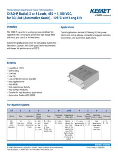
Printed Circuit Board Mount Power Film Capacitors C4AQ-P ...
content.kemet.comB x H x L (mm) Tolerance C4 = MKP dimensions power capacitors A = Box, wire terminals Q = DC link Automotive Grade G = 450 H = 600 J = 700 O = 900 Q = 1,100 B, E = Box plastic case L = Low Profile box, plastic case U = 2 pins W = 4 pins Digits 2 – 4 indicate the first three digits of the capacitance value. First digit indicates the number
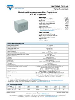
Metallized Polypropylene Film Capacitors DC-Link Capacitor
www.vishay.comMetallized Polypropylene Film Capacitors DC-Link Capacitor FEATURES • High performance DC filter •Low ESR • High peak current capabilities • High RMS current capabilities ... 52.5 Y h w Ø dt I 6 - 1 P1 ± 0.4 - PCM 27.5 mm P1 ± 0.5 - PCM ≥ 37.5 mm P1 P1 ± 0.5 Marking I w 6 - 2 Ø dt P2 ± 0.5 h P1 P2 P2. MKP1848 DC-Link

Surface Mount Multilayer Ceramic Chip Capacitors (SMD ...
content.kemet.comX = 10 Y = 16 Z = 25 A = 50 B = 100 Two significant digits and number of zeros. J = ±5% K = ±10% M = ±20% D = Sn/Pb solder dipped G = Nickel gold-plating R = Flexible termination with solder plating V = Flexible termination with nickel gold-plating Z = Sn/Pb solder plated M = M Level T = T Level B = BME

Lecture 13 Linear dynamical systems with inputs & outputs
see.stanford.edu• output is state: y = x • unit resistors, unit capacitors • step response matrix shows delay to each node Linear dynamical systems with inputs & outputs 13–14. system is
Science Bowl Questions/Answers for Physics
www.csun.edux) The magnitude of the charge is the same on all of the capacitor plates. y) The capacitance of the system depends on the voltage applied across the three capacitors. ANSWER: X -- THE MAGNITUDE OF THE CHARGE IS THE SAME ON ALL OF THE CAPACITOR PLATES PHYS-91; Multiple Choice: For a parallel-plate capacitor with plate area "A" and plate

INTRODUCTION TO DIGITAL FILTERS - Physics 123/253
123.physics.ucdavis.eduy n = x n-1 The output value at time t = nh is simply the input at time t = (n-1)h, i.e. the signal is delayed by time h: y = x y = x y = x y = x... etc 0 -1 1 0 2 1 3 2 Note that as sampling is assumed to commence at t = 0, the input value x-1 at t = -h is undefined. It is usual to take this (and any other values of x …

Sub-threshold MOSFET Operation - MIT OpenCourseWare
ocw.mit.eduy v BS = 0 B x y 0 L -So far this is standard MOSFET operating procedure. We could apply a positive voltage to the gate and when it was larger than V T we would see the normal drain current that we modeled earlier. Rather than do this, however, consider forward biasing the substrate-source diode junction, I.e, v BS > 0…