Transcription of Bootstrap Circuit in the Buck Converter
1 1/4 2017 ROHM Co., Ltd. No. 60AP001E Application Note 2018 ROHM Co., Ltd. No. 61AN073E Switching Regulator IC Series Bootstrap Circuit in the Buck Converter This application note explains the step-up Circuit using a Bootstrap capacitor. In buck converters, this Circuit is used when the high-side switch is the N-ch Role of the Bootstrap Circuit in the buck Converter The configuration of the Circuit in proximity to a buck Converter depends on the polarity of the high-side switch. When a P-ch MOSFET is used for the high-side switch, there are advantages over using a N-ch MOSFET, such as the capability of driving the switch with input voltage VIN as the gate voltage, as well as voltage reduction and obtainment of the maximum duty. On the contrary, the use of a P-ch MOSFET requires a larger chip area for passing the same current. The use of an N-ch MOSFET for the high-side switch requires a gate voltage of VIN + Vth (threshold voltage of the N-ch MOSFET) or higher.
2 A step-up Circuit is required because the gate voltage is higher than VIN. This Circuit is configured with an internal diode and an external Bootstrap capacitor (charge pump type). The total cost, including the cost of the external Bootstrap capacitor, can be lowered because the chip area can be reduced compared with the P-ch MOSFET, as mentioned above. 2. Description of the charge pump operation In the charge-pump-type step-up Circuit , the essential parts include a diode and a capacitor ( Bootstrap capacitor). The diode is often built-in as an element in the IC, and only the Bootstrap capacitor is connected externally. Figure 1 shows an example of an actual capacitorBuilt-in diodeHigh-side switchNch MOSFETVINSWBOOTVING roundElements in the ICVOUTVINLow-side switchNch MOSFET Figure 1. Example of a charge-pump-type step-up Circuit The voltages on the SW and BOOT pins in the example of Figure 1 are described as shown in Figure 2, where Vf is the forward direction voltage of the built-in diode.
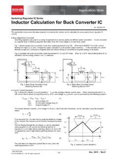
3 GroundVIN2 VIN2 VIN-VfVIN-VfSW VoltageBOOT Voltage Figure 2. Voltages of SW and BOOT 2/4 Application Note Bootstrap Circuit in the Buck Converter 2018 ROHM Co., Ltd. No. 61AN073E When the SW voltage is low during the switching operations in Figure 2, the electric charge is stored in the capacitor from VIN, thus resulting in the voltage of VIN - Vf across the capacitor. When the SW voltage is high, the BOOT voltage increases up to 2 VIN - Vf, and the built-in diode maintains the voltage at 2 VIN - Vf. Therefore, the BOOT voltage switches between VIN - Vf and 2 VIN - Vf (Figure 3). BOOT=VIN-Vf[V]VINSWG iven that the VIN voltage > BOOT voltage,a forward direction current flows in the SW = Ground, the BOOT voltage is VIN - Vf [V]. When the SW voltage is lowBOOT=2 VIN-Vf[V]VINSWG iven that the VIN voltage the BOOT voltage,no current flows in the diode. The voltage acrossthe capacitor is maintained at VIN - Vf [V].
4 Therefore, the BOOT voltage is 2 VIN - Vf [V] when SW = VIN. When the SW voltage is highVING roundVIN-Vf[V]VIN-Vf[V] Figure 3. Charge-pump-type step-up Circuit diagram When this BOOT voltage is used as the gate voltage for the high-side N-ch MOSFET, you can obtain a voltage between the gate and the source (VGS) that is sufficient to completely turn ON the MOSFET. In this example, the anode of the built-in diode is obtained from VIN, and the BOOT voltage can increase up to 2 VIN - Vf as described in the calculation. It is possible that this BOOT voltage may exceed the breakdown voltage between the gate and source of the high-side N-ch MOSFET. Therefore, in designing products with a high input voltage, an internal power supply of approximately 5 V is connected to the anode so that the BOOT voltage is maintained below the breakdown voltage between the gate and the source (Figure 4).
5 BOOTSWVINWhen the anode of the diode is obtained from VIN,the gate voltage of the high-side N-ch MOSFET isVIN - Vf [V] at maximum. When a high voltage isapplied to VIN and when the VGS rating is exceeded,the high-side N-ch MOSFET will be the anode of the diode is connected toan internal power supply of approximately 5 V,the gate voltage of the high-side N-ch MOSFET is5 - Vf [V] at maximum. Therefore, the VGS rating ofthe N-ch MOSFET will not be exceeded,and the high-side N-ch MOSFET can be power supply(5V) Figure 4. Method that considers preventing the VGS rating from being exceeded 3/4 Application Note Bootstrap Circuit in the Buck Converter 2018 ROHM Co., Ltd. No. 61AN073E 3. Capacitance of the Bootstrap capacitor For the minimum capacitance of the Bootstrap capacitors , follow the capacitance described in each data sheet. Use a small ceramic capacitor for the Bootstrap capacitors .
6 It is necessary to consider the DC bias characteristics of the ceramic capacitors and to confirm that the actual capacitance corresponds with the capacitance described in the data sheet. The DC bias characteristics refer to the characteristics of variation in capacitance due to the DC voltage applied across the ceramic capacitor. Generally, the capacitance tends to decrease as the DC voltage increases. Furthermore, the variation in capacitance also depends on the size. Figure 5 shows the examples of DC bias characteristics with different sizes. Figure 5. Examples of DC bias characteristics of ceramic capacitors When 16 V is applied to the 1005 size ceramic capacitor, the actual capacitance falls significantly below the nominal value of F. Furthermore, approximately half of the nominal value remains. Although the minimum capacitance of the Bootstrap capacitor varies with each IC, an excessively small capacitance may result in an electric charge that is insufficient for gate driving.
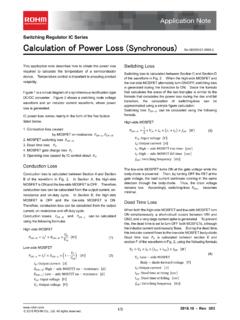
7 The insufficient electric charge may lead to unstable gate driving and impair the operation. However, we recommend the use of the minimum capacitor that satisfies the minimum capacitance because a larger size will affect the cost. On the contrary, an excessively large capacitance could delay the increase in the voltage across the capacitor and reduce the voltage for gate driving. The adequate value of the capacitance can be obtained from the following equations. When the high-side N-ch MOSFET is ON, the electric charge stored in the Bootstrap capacitor is consumed for the gate driving. QLOSS=QG+IBOOT Df QLOSS: Total electric charge consumed when N ch MOSFET is ON QG: Gate charge and electric charge lost in the internal Circuit IBOOT: Current passing from the Bootstrap capacitor f: Switching frequency D: Switching duty Here, the relation of the variation in the voltage between BOOT and SW ( VBS), the capacitance of the Bootstrap capacitor (CBOOT), and the QLOSS is expressed as follows.
8 CBOOT QLOSS VBS Considering that it is desirable to maintain VBS at V or below, the equation can be described as follows. CBOOT 0481216 Capacitance[F]DC Bias Voltage[V]1005 size, F 1608 size, F (1) (2) (3) 4/4 Application Note Bootstrap Circuit in the Buck Converter 2018 ROHM Co., Ltd. No. 61AN073E VINVINCBOOTHigh-sideNch MOSFETBOOTHGSWL evel shifterblockElementsin the ICIBOOT Figure 6. Circuit diagram required for CBOOT determination As an example, a calculation is performed with QG = 10 nC, IBOOT = 10 nA, D = , and f = 1 MHz. From Equation (1), QLOSS=10nC+10nA 10nC When this value is substituted in Equation (3), CBOOT F Therefore, CBOOT should be F or larger. However, the capacitances described in the data sheet should be used because they are designed according to the results obtained from these equations. 5 %ZZZ URKP FRP 6 52+0 &R /WG $OO ULJKWV UHVHUYHG NoticeROHM Customer Support System you for your accessing to ROHM product informations.
9 More detail product informations and catalogs are available, please contact us. Notes The information contained herein is subject to change without notice. Before you use our Products, please contact our sales representative and verify the latest specifica-tions :Although ROHM is continuously working to improve product reliability and quality, semicon-ductors can break down and malfunction due to various , in order to prevent personal injury or fire arising from failure, please take safety measures such as complying with the derating characteristics, implementing redundant and fire prevention designs, and utilizing backups and fail-safe procedures. ROHM shall have no responsibility for any damages arising out of the use of our Poducts beyond the rating specified by of application circuits, Circuit constants and any other information contained herein are provided only to illustrate the standard usage and operations of the Products.
10 The peripheral conditions must be taken into account when designing circuits for mass technical information specified herein is intended only to show the typical functions of and examples of application circuits for the Products. ROHM does not grant you, explicitly or implicitly, any license to use or exercise intellectual property or other rights held by ROHM or any other parties. ROHM shall have no responsibility whatsoever for any dispute arising out of the use of such technical Products specified in this document are not designed to be radiation use of our Products in applications requiring a high degree of reliability (as exemplified below), please contact and consult with a ROHM representative : transportation equipment ( cars, ships, trains), primary communication equipment, traffic lights, fire/crime prevention, safety equipment, medical systems, servers, solar cells, and power transmission not use our Products in applications requiring extremely high reliability, such as aerospace equipment, nuclear power control systems, and submarine shall have no responsibility for any damages or injury arising from non-compliance with the recommended usage conditions and specifications contained has used reasonable care to ensurH the accuracy of the information contained in this document.