Transcription of Datasheet - LMV321, LMV358, LMV324 - Low cost, low power ...
1 October 2015 DocID11887 Rev 8 1/17 This is information on a product in full production. LMV321, LMV358, LMV324 Low cost, low power , input / output rail -to- rail operational amplifiers Datasheet - production data Features Operating range from VCC = to 6 V rail -to- rail input and output Extended Vicm (VDD - V to VCC + V) Low supply current (145 A) Gain bandwidth product (1 MHz) ESD tolerance (2 kV) Related products See LMV321L, LMV358L, LMV324L for newer technological version See TSV851, TSV852, TSV854 for enhanced performances Applications Battery powered electronic equipment Personal medical care (glucose meters) Laptops Description The LMV321/358/324 family (single, dual, and quad)
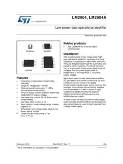
2 Answers the need for low cost, general-purpose operational amplifiers. They operate with voltages as low as V and feature both input and output rail -to- rail , 145 A consumption current, and 1 MHz gain bandwidth product (GBP). With such a low consumption and a sufficient GBP for many applications, these op amps are well suited for any kind of battery supplied and portable equipment application. The LMV321 device is housed in the space-saving 5-pin SOT23-5 package, which simplifies board design. The SOT23-5 has two pinning configurations to answer all application requirements. LMV321 ILT(SOT23-5)LMV358ID/IDT-LMV358 IPT(SO8,TSSOP8)LMV324ID/IDT- LMV324 IPT(SO14,TSSOP14)LMV321 RILT(SOT23-5)Contents LMV321, LMV358, LMV324 2/17 DocID11887 Rev 8 Contents 1 Absolute maximum ratings and operating conditions.
3 3 2 Electrical characteristics .. 5 3 Package information .. 9 SOT23-5 package information .. 10 SO8 package information .. 11 TSSOP8 package information .. 12 SO14 package information .. 13 TSSOP14 package information .. 14 4 Ordering information .. 15 5 Revision history .. 16 LMV321, LMV358, LMV324 Absolute maximum ratings and operating conditions DocID11887 Rev 8 3/17 1 Absolute maximum ratings and operating conditions Table 1: Absolute maximum ratings Symbol Parameter Value Unit VCC Supply voltage (1) 7 V Vid Differential input voltage (2) 1 Vin input voltage VDD - to VCC + Toper Operating free air temperature range -40 to 125 C Tstg Storage temperature -65 to 150 Tj Maximum junction temperature 150 Rthja Thermal resistance junction-to-ambient (3) SOT23-5 250 C/W SO8 125 TSSOP8 120 SO14 103 TSSOP14 100 Rthjc Thermal resistance junction-to-case(3) SOT23-5 81 SO8 40 TSSOP8 37 SO14 31 TSSOP14 32 ESD HBM.
4 Human body model (4) 2 kV MM: machine model (5) 200 V CDM: charged device model (6) kV Lead temperature (soldering, 10 s) 250 C output short-circuit duration See (7) Notes: (1)All voltage values, except differential voltage are with respect to network terminal. (2)The differential voltage is the non-inverting input terminal with respect to the inverting input terminal. If Vid > 1 V, the maximum input current must not exceed 1 mA. In this case (Vid > 1 V), an input series resistor must be added to limit input current. (3)Short-circuits can cause excessive heating. Destructive dissipation can result from simultaneous short-circuits on all amplifiers. All values are typical.
5 (4)Human body model: a 100 pF capacitor is charged to the specified voltage, then discharged through a k resistor between two pins of the device. This is done for all couples of connected pin combinations while the other pins are floating. (5)Machine model: a 200 pF capacitor is charged to the specified voltage, then discharged directly between two pins of the device with no external series resistor (internal resistor < 5 ). This is done for all couples of connected pin combinations while the other pins are floating. (6)Charged device model: all pins and the package are charged together to the specified voltage and then discharged directly to the ground through only one pin.
6 This is done for all pins. No value specified for CDM on SOT23-5 package. The value is given for SO8 and TSSOP packages. (7)Short-circuits from the output to VCC can cause excessive heating. The maximum output current is approximately 48 mA, independent of the magnitude of VCC. Destructive dissipation can result from simultaneous short-circuits on all amplifiers. Absolute maximum ratings and operating conditions LMV321, LMV358, LMV324 4/17 DocID11887 Rev 8 Table 2: Operating conditions Symbol Parameter Value Unit VCC Supply voltage to 6 V Vicm Common mode input voltage range (1) VDD - to VCC + Vicm Common mode input voltage range (2) VDD to VCC Toper Operating free air temperature range -40 to 125 C Notes: (1)At 25 C, for VCC 6 V, Vicm is extended to VDD - V, VCC + V.
7 (2)In full temperature range, both rails can be reached when VCC does not exceed V. LMV321, LMV358, LMV324 Electrical characteristics DocID11887 Rev 8 5/17 2 Electrical characteristics Table 3: Electrical characteristics at VCC = V, VDD = 0 V, CL and RL connected to VCC/2, Tamb = 25 C (unless otherwise specified) Symbol Parameter Conditions Min. Typ. Max. Unit Vio input offset voltage Vicm = Vout = VCC/2 3 mV Tmin Tamb Tmax 6 Vio/ T input offset voltage drift 2 V/ C Iio input offset current Vicm = Vout = VCC/2 (1) 1 9 nA Tmin Tamb Tmax 25 Iib input bias current Vicm = Vout = VCC/2 (1) 10 50 Tmin Tamb Tmax 85 CMR Common mode rejection ratio 0 Vicm VCC 55 85 dB SVR Supply voltage rejection ratio Vicm = VCC/2 70 80 Avd Large signal voltage gain Vout = V to V, RL = 10 k 80 100 Vout = V to V, RL = 2 k 70 88 VOH High level output voltage Vid = 100 mV, Tmin Tamb Tmax, RL = 10 k V Vid = 100 mV, Tmin Tamb Tmax, RL = 2 k VOL Low level output voltage Vid = -100 mV, Tmin Tamb Tmax, RL = 10 k 15 90 mV Vid = -100 mV, Tmin Tamb Tmax, RL = 2 k 50 100 Io output current output source current, Vid = 100 mV, VO = VDD 5 46 mA output sink current, Vid = -100 mV.
8 VO = VCC 5 46 ICC Supply current (per amplifier) Vout = VCC/2, AVCL = 1, no load 145 200 A Tmin Tamb Tmax 230 GBP Gain bandwidth product RL = 10 k , CL = 100 pF, f = 100 kHz 1 MHz SR Slew rate RL = 600 , CL = 100 pF, AV = 1 V/ s m Phase margin RL = 600 , CL = 100 pF 44 Degrees en input voltage noise 40 nV/ Hz THD Total harmonic distortion % Notes: (1)Maximum values include unavoidable inaccuracies of the industrial tests. Electrical characteristics LMV321, LMV358, LMV324 6/17 DocID11887 Rev 8 Table 4: Electrical characteristics at VCC = 5 V, VDD = 0 V, CL and RL connected to VCC/2, Tamb = 25 C (unless otherwise specified) Symbol Parameter Conditions Min.
9 Typ. Max. Unit Vio input offset voltage Vicm = Vout = VCC/2 3 mV Tmin Tamb Tmax 6 Vio/ T input offset voltage drift 2 V/ C Iio input offset current Vicm = Vout = VCC/2 (1) 1 9 nA Tmin Tamb Tmax 25 Iib input bias current Vicm = Vout = VCC/2 (1) 16 63 Tmin Tamb Tmax 95 CMR Common mode rejection ratio 0 Vicm VCC 65 95 dB SVR Supply voltage rejection ratio Vicm = VCC/2 70 90 Avd Large signal voltage gain Vout = V to V, RL = 10 k 85 97 Vout = V to V, RL = 2 k 77 93 VOH High level output voltage Vid = 100 mV, Tmin Tamb Tmax, RL = 10 k V Vid = 100 mV, Tmin Tamb Tmax, RL = 2 k VOL Low level output voltage Vid = -100 mV, Tmin Tamb Tmax, RL = 10 k 40 180 mV Vid = -100 mV, Tmin Tamb Tmax, RL = 2 k 80 200 Io output current output source current, Vid = 100 mV, VO = VDD 7 48 mA output sink current, Vid = -100 mV.
10 VO = VCC 7 48 ICC Supply current (per amplifier) Vout = VCC/2, AVCL = 1, no load 162 220 A Tmin Tamb Tmax 250 GBP Gain bandwidth product RL = 10 k , CL = 100 pF, f = 100 kHz MHz SR Slew rate RL = 600 , CL = 100 pF, AV = 1 V/ s m Phase margin RL = 600 , CL = 100 pF 48 Degrees en input voltage noise 40 nV/ Hz THD Total harmonic distortion % Notes: (1)Maximum values include unavoidable inaccuracies of the industrial tests. LMV321, LMV358, LMV324 Electrical characteristics DocID11887 Rev 8 7/17 Figure 1: Supply current/amplifier vs. supply voltage Figure 2: input bias current vs. temperature (VCC = 3 V, Vicm = V) Figure 3: input bias current vs.
