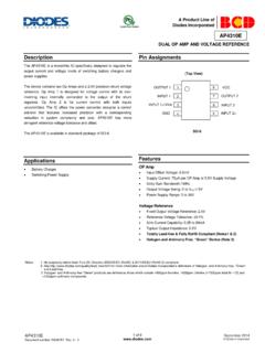
Transcription of Description Pin Assignments - Diodes Incorporated
1 74HC138 Document number: DS35488 - 2 1 of 10 June 2013 Diodes Incorporated 74HC1383 TO 8 LINE DECODER DEMULTIPLEXER Description The 74HC138 is a high speed CMOS device. The device accepts a three bit binary weighted address on input pins A0, A1 and A2 and when enabled will produce one active low output with the remaing seven being high. There are two active LOW enable inputs E1 and E2, and one active HIGH enable input E3. The disabled device state results in all outputs being high. The enable state occurs with E1 and E2 asserted low and E3 asserted high. The multiple enable lines allow for the parallel expansion of decoders to create 4-to-16 line versions with no additional parts and 5-to-32 versions with the addition of a single inverter.
2 Features Wide Supply Voltage Range from to Sinks or sources 8 mA at VCC = CMOS low power consumption Schmitt Trigger Action at All Inputs Inputs Accept up to ESD Protection Tested per JESD 22 Exceeds 200-V Machine Model (A115-A) Exceeds 2000-V Human Body Model (A114-A) Exceeds 1000-V Charged Device Model (C101C) Latch-Up Exceeds 100mA per JESD 78D, Class II Totally Lead-Free & Fully RoHS Compliant (Notes 1 & 2) Halogen and Antimony Free. Green Device (Note 3) Pin Assignments Applications Memory chip select decoding Demultiplexing Single line peripheral control Allow simple serial bit streams from a microcontroller to control as many peripheral lines as needed Notes: 1.
3 No purposely added lead. Fully EU Directive 2002/95/EC (RoHS) & 2011/65/EU (RoHS 2) compliant. 2. See for more information about Diodes Incorporated s definitions of Halogen- and Antimony-free, "Green" and Lead-free. 3. Halogen- and Antimony-free "Green products are defined as those which contain <900ppm bromine, <900ppm chlorine (<1500ppm total Br + Cl) and <1000ppm antimony compounds. Click here for ordering information, located at the end of datasheet 74HC138 Document number: DS35488 - 2 2 of 10 June 2013 Diodes Incorporated 74HC138 Pin descriptions Pin Number Pin Name Description 1 A0 Address Input 0 2 A1 Address Input 1 3 A2 Address Input 2 4 E1 Enable Input 1 (active LOW) 5 E2 Enable Input 2 (active LOW) 6 E3 Enable Input 3 (active HIGH) 7 Y7 Output 7 (active LOW) 8 GND Ground 9 Y6 Output 6 (active LOW) 10 Y5 Output 5 (active LOW) 11 Y4 Output 4 (active LOW) 12 Y3 Output 3 (active LOW) 13 Y2 Output 2 (active LOW) 14 Y1 Output 1 (active LOW) 15 Y0 Output o (active LOW)
4 16 Vcc Supply Voltage Function Table Diagram Control Input Output E1 E2 E3 A2 A1 A0 Y7 Y6 Y5 Y4 Y3 Y2 Y1 Y0 H X X X X X H H H H H H H H X H X X X L L L H L L L H H H H H H H L L L H H H H H H H L H L H L H H H H H L H H L H H H H H H
5 L H H H H L L H H H L H H H H H L H H H L H H H H H H H L H L H H H H H H H H H L H H H H H H H 74HC138 Document number: DS35488 - 2 3 of 10 June 2013 Diodes Incorporated 74HC138 Logic Diagram 74HC138 Document number: DS35488 - 2 4 of 10 June 2013 Diodes Incorporated 74HC138 Absolute Maximum Ratings (Note 4) (@TA = +25 C, unless otherwise specified.)
6 Symbol Description Rating Unit ESD HBM Human Body Model ESD Protection 2 kV ESD CDM Charged Device Model ESD Protection 1 kV ESD MM Machine Model ESD Protection 200 V VCC Supply Voltage Range to + V VI Input Voltage Range to + V Vo Voltage applied to output in high or low state to VCC + V IIK Input Clamp Current VI< -20 mA IIK Input Clamp Current VI > VCC + 20 mA IOK Output Clamp Current VO< -20 mA IOK Output Clamp Current VO> VCC + 20 mA IO Continuous output current 25 mA ICC Continuous current through VCC 50 mA IGND Continuous current through GND -50 mA TJ Operating Junction Temperature -40 to +150 C TSTG Storage Temperature -65 to +150 C PTOT Total Power Dissipation 500 mW Note: 4.
7 Stresses beyond the absolute maximum may result in immediate failure or reduced reliability. These are stress values and device operation should be within recommend values. Recommended Operating Conditions (Note 5) (@TA = +25 C, unless otherwise specified.) Symbol Parameter Conditions Min Max Unit VCC Supply Voltage V VI Input Voltage 0 VCC V VO Output Voltage Active Mode 0 VCC V t/ V Input transition Rise or Fall Rate VCC = 1000 ns/V VCC = 500 VCC = 400 TA Operating Free-Air Temperature -40 +125 C Note: 5.
8 Unused inputs should be held at VCC or Ground. 74HC138 Document number: DS35488 - 2 5 of 10 June 2013 Diodes Incorporated 74HC138 Electrical Characteristics (@TA = +25 C, unless otherwise specified.) Symbol Parameter Test Conditions VCC TA = +25 C TA = -40 C to +85 C TA = -40 C to +125 C UnitMin Typ MaxMin Max Min Max VIH High-Level Input Voltage V VIL Low-Level Input Voltage V VOH High-Level Output Voltage IOH = -20 A All outputs V IOH = -4 mA IOH = mA VOL Low-Level Output Voltage IOL = 20 A All outputs 0 V 0 0 IOL = 4 mA IOL = mA II Input
9 Current VI =GND or 1 1 A ICC Supply Current VI = GND or VCC IO = 0 80 160 A Ci Input Capacitance Vi = VCC or GND 4 10 10 10 pF Switching Characteristics Symbol / Parameter Pins Test Conditions VCC TA = +25 C -40 C to +85 C -40 C to +125 C Unit Min Typ Max Min Max Min Max tPLH, tPLH Propagation Delay An to Yn Figure 1 41 150 190 225 ns 15 30 38 45 12 12 26 33 38 E3 to Yn Figure 1 47 150 190 225 17 30 38 45 14 14 26 33 38 En to Yn Figure 1 47 150 190 225 17 30 38 45 14 14 26 33 38 tTLH, tTHL Transition Time Yn Figure 1 19 75 95 110 ns 7 15 19 22 6 13 16 19 74HC138 Document number.
10 DS35488 - 2 6 of 10 June 2013 Diodes Incorporated 74HC138 Operating Characteristics (@TA = +25 C, unless otherwise specified.) Parameter Test Conditions VCC = 5V Unit Typ Cpd Power dissipation capacitance f = 1 MHz all outputs switching-no load 19 pF Parameter Measurement Information Vcc Inputs VM CL VI tr/tf VCC 6 ns VCC/2 50pF VCC 6 ns VCC/2 15pF used for 5V typical test Voltage Waveform Pulse Duration Voltage Waveform Propagation Delay Times Inverting and Non Inverting Outputs Notes: A. Includes test lead and test apparatus capacitance. B.