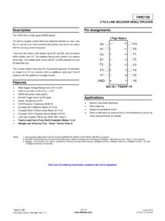
Transcription of Description Pin Assignments - Diodes Incorporated
1 AP4310E Document number: DS36787 Rev. 3 - 2 1 of 9 September 2014 Diodes Incorporated AP4310E A Product Line of Diodes Incorporated DUAL OP AMP AND VOLTAGE REFERENCE Description The AP4310E is a monolithic IC specifically designed to regulate the output current and voltage levels of switching battery chargers and power supplies The device contains two Op Amps and a precision shunt voltage reference. Op Amp 1 is designed for voltage control with its non-inverting input internally connected to the output of the shunt regulator. Op Amp 2 is for current control with both inputs uncommitted. The IC offers the power converter designer a control solution that features increased precision with a corresponding reduction in system complexity and cost.
2 AP4310E has more stringent reference voltage tolerance and offset. The AP4310E is available in standard package of SO-8. Applications Battery Charger Switching Power Supply Pin Assignments (Top View) 12348765 OUTPUT 1 INPUT 1-INPUT 1+/VKAGNDINPUT 2-INPUT 2+OUTPUT 2 VCC SO-8 Features OP Amp Input Offset Voltage: Supply Current: 75 A per OP Amp at Supply Voltage Unity Gain Bandwidth:1 MHz Output Voltage Swing: 0 to Power Supply Range: 3 to 36V Voltage Reference Fixed Output Voltage Reference: Reference Voltage Tolerance: Sink Current Capability: to 80mA Typical Output Impedance: Totally Lead-free & Fully RoHS Compliant (Notes1 & 2) Halogen and Antimony Free. Green Device (Note 3) Notes: 1.
3 No purposely added lead. Fully EU Directive 2002/95/EC (RoHS) & 2011/65/EU (RoHS 2) compliant. 2. See for more information about Diodes Incorporated s definitions of Halogen- and Antimony-free, "Green" and Lead-free. 3. Halogen- and Antimony-free "Green products are defined as those which contain <900ppm bromine, <900ppm chlorine (<1500ppm total Br + Cl) and <1000ppm antimony compounds. AP4310E Document number: DS36787 Rev. 3 - 2 2 of 9 September 2014 Diodes Incorporated AP4310E A Product Line of Diodes Incorporated Typical Applications Circuit AC LineSMPSR2 Current SenseR7R8 Battery PackR4R3R5R6R1 OptoIsolator+-Op Amp 2+-Op Amp 1AP4310 EVREF Application of AP4310E in a Constant Current and Constant Voltage Charger Functional Block Diagram -+-+12348765 OpAmp 1 OpAmp 2 OUTPUT 1 INPUT 1-INPUT 1+/VKAGNDVCCOUTPUT 2 INPUT 2-INPUT 2+VREF AP4310E Document number: DS36787 Rev.
4 3 - 2 3 of 9 September 2014 Diodes Incorporated AP4310E A Product Line of Diodes Incorporated Absolute Maximum Ratings (Note 4) Symbol Parameter Rating Unit VCC Power Supply Voltage (VCC to GND) 40 V VIN Op Amp1 and 2 Input Voltage Range (Pins 2, 5, 6) to VCC+ V VID Op Amp 2 Input Differential Voltage (Pins 5, 6) 40 V IK Voltage Reference Cathode Current (Pin 3) 100 mA PD Power Dissipation (TA=+25 C) 500 mW TJ Operating Junction Temperature +150 C TSTG Storage Temperature Range -65 to +150 C TLEAD Lead Temperature (Soldering 10sec) +260 C Note 4: Stresses greater than those listed under Absolute Maximum Ratings may cause permanent damage to the device. These are stress ratings only, and functional operation of the device at these or any other conditions beyond those indicated under Recommended Operating Conditions is not implied.
5 Exposure to Absolute Maximum Ratings for extended periods may affect device reliability. Recommended Operating Conditions (Note 5) Parameter Min Max Unit Supply Voltage 3 36 V Ambient Temperature -40 +105 C Note 5: Qualified for SMD on the underside of a PCB by processing the PCB through a wave soldering operation. Electrical Characteristics (@VCC=5V, TA=+25 C, unless otherwise specified.) Parameters Conditions Min Typ Max Unit Total Supply Current, excluding Current in Voltage Reference VCC=5V, no load, -40 C TA +105 C mA VCC=30V, no load, -40 C TA +105 C Voltage Reference Section Reference Voltage IK=10mA TA=+25 C V -40 C TA +105 C Reference Voltage Deviation over Full Temperature Range IK=10mA, TA=-40 C to +105 C 5 24 mV Minimum Cathode Current for Regulation mA Dynamic Impedance IK=1mA to 80mA, f<1kHz Op Amp 1 Section (VCC=5V, VO= , TA=+25 C, unless otherwise noted.)
6 Input Offset Voltage TA=+25 C 3 mV TA=-40 C to +105 C 5 Input Offset Voltage Temperature Drift TA=-40 C to +105 C 7 V/ C Input Bias Current (Inverting Input Only) TA=+25 C 20 150 nA Large Signal Voltage Gain VCC=15V, RL=2k VO= to 85 100 dB Power Supply Rejection Ratio VCC=5V to 30V 70 90 dB AP4310E Document number: DS36787 Rev. 3 - 2 4 of 9 September 2014 Diodes Incorporated AP4310E A Product Line of Diodes Incorporated Electrical Characteristics (Cont.) (@VCC=5V, TA=+25 C, unless otherwise specified.) Parameters Conditions Min Typ Max Unit Output Current Source VCC = 15V, VID=1V VO = 2V 20 40 mA Sink VCC = 15V, VID = -1V VO = 2V 8 20 Output Voltage Swing (High) VCC = 30V, RL = 10k VID = 1V 27 28 V Output Voltage Swing (Low) VCC = 30V, RL = 10k VID = -1V 17 100 mV Slew Rate VCC = 18V, RL = 2k AV = 1, VIN = to 2V, CL = 100pF V/ s Unity Gain Bandwidth VCC = 30V, RL = 2k CL = 100pF MHz Op Amp 2 Section (VCC= 5V, VO= , TA =+25 C, unless otherwise noted.)
7 Input Offset Voltage (Note 6) TA = +25 C, VCC = 5V or 20V 2 mV TA = -40 C to +105 C, VCC = 5V or 20V 3 Input Offset Voltage Temperature Drift TA = -40 C to +105 C 7 V/ C Input Offset Current TA = +25 C 2 30 nA Input Bias Current TA = +25 C 20 150 nA Input Voltage Range VCC = 0 to 36V 0 V Common Mode Rejection Ratio TA = +25 C, VCM = 0 to 70 85 dB Large Signal Voltage Gain VCC = 15V, RL = 2k VO = to 85 100 dB Power Supply Rejection Ratio VCC = 5V to 30V 70 90 dB Output Current Source VCC = 15V, VID = 1V VO = 2V 20 40 mA Sink VCC = 15V, VID = -1V VO = 2V 8 20 Output Voltage Swing (High) VCC = 30V, RL = 10k VID = 1V 27 28 V Output Voltage Swing (Low) VCC = 30V, RL = 10k VID = -1V 17 100 mV Slew Rate VCC = 18V, RL = 2k AV = 1, VIN = to 2V, CL = 100pF V/ s Unity Gain Bandwidth VCC = 30V, RL = 2k CL = 100pF MHz Note 6: The full temperature feature is guaranteed by design.
8 AP4310E Document number: DS36787 Rev. 3 - 2 5 of 9 September 2014 Diodes Incorporated AP4310E A Product Line of Diodes Incorporated Performance Characteristics Reference Voltage vs. Ambient Temperature Cathode Current vs. Cathode Voltage Input Bias Current vs. Ambient Temperature Op Amp Voltage Gain Voltage (V)Ambient Temperature (oC)-2-10123-100-50050100150 Cathode Current (mA)Cathode Voltage (V)VKA=VREFTA=250C-40-200204060801001200 51015202530 Input Bias Current (nA)Ambient Temperature (oC)0246810121416182060708090100110 Voltage Gain(dB)Supply Voltage (V) RL=2K RL=20K AP4310E Document number: DS36787 Rev.
9 3 - 2 6 of 9 September 2014 Diodes Incorporated AP4310E A Product Line of Diodes Incorporated Ordering Information AP4310E X XX - G1 PackingPackageTR : Tape & ReelM: SO-8G1 : GreenRoHS/GreenProduct Name Package Temperature Range Reference Voltage Voltage Tolerance Part Number Marking ID Packing SO-8 -40 to +105 C AP4310 EMTR-G1 AP4310EM-G1 4000/Tape & Reel Marking Information (Top View) First and Second Lines: Logo and Marking ID Third Line: Date Code Y: Year WW: Work Week of Molding A: Assembly House Code XX: 7th and 8th Digits of Batch No. AP4310 EM-G1 YWWAXX- AP4310E Document number: DS36787 Rev. 3 - 2 7 of 9 September 2014 Diodes Incorporated AP4310E A Product Line of Diodes Incorporated Package Outline Dimensions (All dimensions in mm (inch).)
10 (1) Package Type: SO-8 0 8 1 7 ( ) ( ) ( ) ( ) ( ) ( ) ( ) ( ) ( ) ( ) ( )7 7 20 ( ) ( ) ( )8 ( ) ( ) ( ) ( ) ( )8 ( ) ( ) ( ) ( )Note: Eject hole, oriented hole and mold mark is 1 Option 1 Option ( )TYPTYPTYP9 ~9 ~ AP4310E Document number: DS36787 Rev. 3 - 2 8 of 9 September 2014 Diodes Incorporated AP4310E A Product Line of Diodes Incorporated Suggested Pad Layout (1) Package Type: SO-8 GridplacementcourtyardZGYEX Dimensions Z (mm)/(inch) G (mm)/(inch) X (mm)/(inch) Y (mm)/(inch) E (mm)/(inch) Value AP4310E Document number: DS36787 Rev. 3 - 2 9 of 9 September 2014 Diodes Incorporated AP4310E A Product Line of Diodes Incorporated IMPORTANT NOTICE Diodes Incorporated MAKES NO WARRANTY OF ANY KIND, EXPRESS OR IMPLIED, WITH REGARDS TO THIS DOCUMENT, INCLUDING, BUT NOT LIMITED TO, THE IMPLIED WARRANTIES OF MERCHANTABILITY AND FITNESS FOR A PARTICULAR PURPOSE (AND THEIR EQUIVALENTS UNDER THE LAWS OF ANY JURISDICTION).