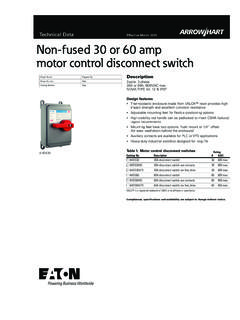
Transcription of Differential current outputs: 2 mA to 20 mA …
1 14-Bit, 210 MSPS TxDAC . D/A Converter Data Sheet ad9744 . FEATURES APPLICATIONS. High performance member of pin-compatible Wideband communication transmit channel TxDAC product family Direct IFs Excellent spurious-free dynamic range performance Base stations SFDR to Nyquist Wireless local loops 83 dBc at 5 MHz output Digital radio links 80 dBc at 10 MHz output Direct digital synthesis (DDS). 73 dBc at 20 MHz output Instrumentation SNR at 5 MHz output, 125 MSPS: 77 dB. Twos complement or straight binary data format Differential current outputs: 2 mA to 20 mA FUNCTIONAL BLOCK DIAGRAM. Power dissipation: 135 mW at V Power-down mode: 15 mW at V. REFLO 150pF AVDD ACOM. On-chip V reference REF. F. CMOS-compatible digital interface REFIO current ad9744 . FS ADJ SOURCE. 28-lead SOIC, 28-lead TSSOP, and 32-lead LFCSP packages ARRAY. Edge-triggered latches RSET DVDD IOUTA. SEGMENTED LSB. DCOM SWITCHES SWITCHES IOUTB. CLOCK. CLOCK LATCHES MODE. 02913-001.
2 DIGITAL DATA INPUTS (DB13 DB0). SLEEP. Figure 1. GENERAL DESCRIPTION. The ad9744 1 is a 14-bit resolution, wideband, third generation Edge-triggered input latches and a V temperature compensated member of the TxDAC series of high performance, low power band gap reference have been integrated to provide a complete CMOS digital-to-analog converters (DACs). The TxDAC family, monolithic DAC solution. The digital inputs support 3 V. consisting of pin-compatible 8-, 10-, 12-, and 14-bit DACs, is CMOS logic families. specifically optimized for the transmit signal path of communi- PRODUCT HIGHLIGHTS. cation systems. All of the devices share the same interface options, small outline package, and pinout, providing an upward or 1. The ad9744 is the 14-bit member of the pin compatible TxDAC. downward component selection path based on performance, family, which offers excellent INL and DNL performance. resolution, and cost. The ad9744 offers exceptional ac and dc 2.
3 Data input supports twos complement or straight binary data performance while supporting update rates up to 210 MSPS. coding. 3. High speed, single-ended CMOS clock input supports The ad9744 's low power dissipation makes it well suited for 210 MSPS conversion rate. portable and low power applications. Its power dissipation can 4. Low power: Complete CMOS DAC function operates on be further reduced to a mere 60 mW with a slight degradation 135 mW from a V to V single supply. The DAC full- in performance by lowering the full-scale current output. Also, scale current can be reduced for lower power operation, and a a power-down mode reduces the standby power dissipation to sleep mode is provided for low power idle periods. approximately 15 mW. A segmented current source architecture 5. On-chip voltage reference: The ad9744 includes a V. is combined with a proprietary switching technique to reduce temperature compensated band gap voltage reference.
4 Spurious components and enhance dynamic performance. 6. Industry-standard 28-lead SOIC, 28-lead TSSOP, and 32-lead LFCSP packages. 1. Protected by Patent Numbers 5568145, 5689257, and 5703519. Rev. C Document Feedback Information furnished by Analog Devices is believed to be accurate and reliable. However, no responsibility is assumed by Analog Devices for its use, nor for any infringements of patents or other rights of third parties that may result from its use. Specifications subject to change without notice. No One Technology Way, Box 9106, Norwood, MA 02062-9106, license is granted by implication or otherwise under any patent or patent rights of Analog Devices. Tel: 2003 2013 Analog Devices, Inc. All rights reserved. Trademarks and registered trademarks are the property of their respective owners. Technical Support ad9744 Data Sheet TABLE OF CONTENTS. Features .. 1 Reference Control Amplifier .. 13. Applications .. 1 DAC Transfer Function.
5 14. Functional Block Diagram .. 1 Analog Outputs .. 14. General Description .. 1 Digital Inputs .. 15. Product Highlights .. 1 Clock 15. Revision History .. 2 DAC 16. 3 Power 16. DC Specifications .. 3 Applying the ad9744 .. 17. Dynamic Specifications .. 4 Differential Coupling Using a 17. Digital Specifications .. 5 Differential Coupling Using an Op Amp .. 17. Absolute Maximum 6 Single-Ended Unbuffered Voltage Output .. 18. Thermal Characteristics .. 6 Single-Ended, Buffered Voltage Output Configuration .. 18. ESD Caution .. 6 Power and Grounding Considerations, Power Supply Pin Configurations and Function Descriptions .. 7 Rejection .. 18. Typical Performance Characteristics .. 8 Evaluation Board .. 20. Terminology .. 12 General Description .. 20. Functional Description .. 13 Outline Dimensions .. 30. Reference Operation .. 13 Ordering 31. REVISION HISTORY. 12/13 Rev. B to Rev. C 5/03 Rev. 0 to Rev. A. Added Table 5; Renumbered Sequentially.
6 6 Added 32-Lead LFCSP Package .. Universal Added Exposed Pad Note to Figure 4 and Table 6, Pin Edits to Configurations and Function Descriptions Section .. 7 Edits to Product Moved Terminology Section .. 12 Edits to DC Specifications ..2. Updated Outline Dimensions .. 30 Edits to Dynamic Specifications ..3. Changes to Ordering Guide .. 31 Edits to Digital Specifications ..4. Edits to Absolute Maximum Ratings ..5. 4/05 Rev. A to Rev. B Edits to Thermal Characteristics ..5. Updated Format .. Universal Edits to Ordering Guide ..5. Changes to General Description .. 1 Edits to Pin Configuration ..6. Changes to Product 1 Edits to Pin Function Descriptions ..6. Changes to DC Specifications .. 3 Edits to Figure 2 ..7. Changes to Dynamic Specifications .. 4 Replaced TPCs 1, 4, 7, and 8 ..8. Changes to Pin Function Description .. 7 Edits to Figure 3 .. 10. Changes to Figure 6 and Figure 9 .. 9 Edits to Functional Description .. 10. Inserted New Figure 10; Renumbered Sequentially.
7 9 Added Clock Input Section .. 12. Changes to Figure 12, Figure 13, Figure 14, and Figure 15 .. 10 Added Figure 7 .. 12. Changes to Figure 22 Caption .. 11 Edits to DAC Timing Section .. 12. Inserted New Figure 23; Renumbered Sequentially .. 11 Edits to Sleep Mode Operation 13. Changes to Functional Description .. 13 Edits to Power Dissipation Section .. 13. Changes to Reference Operation Section .. 13 Renumbered Figures 8 to Figure 26 .. 13. Added Figure 25; Renumbered Sequentially .. 13 Added Figure 11 .. 13. Changes to Digital Inputs Section .. 15 Added Figure 27 to Figure 35 .. 21. Changes to Figure 31 and Figure 16 Updated Outline Dimensions .. 26. Updated Outline Dimensions .. 30. Changes to Ordering Guide .. 31. Rev. C | Page 2 of 32. Data Sheet ad9744 . SPECIFICATIONS. DC SPECIFICATIONS. TMIN to TMAX, AVDD = V, DVDD = V, CLKVDD = V, IOUTFS = 20 mA, unless otherwise noted. Table 1. Parameter Min Typ Max Unit RESOLUTION 14 Bits DC ACCURACY 1.
8 Integral Linearity Error (INL) 5 +5 LSB. Differential Nonlinearity (DNL) 3 +3 LSB. ANALOG OUTPUT. Offset Error + % of FSR. Gain Error (Without Internal Reference) + % of FSR. Gain Error (With Internal Reference) + % of FSR. Full-Scale Output current 2 2 20 mA. Output Compliance Range 1 + V. Output Resistance 100 k . Output Capacitance 5 pF. REFERENCE OUTPUT. Reference Voltage V. Reference Output current 3 100 nA. REFERENCE INPUT. Input Compliance Range V. Reference Input Resistance (External Reference) 7 k . Small Signal Bandwidth MHz TEMPERATURE COEFFICIENTS. Offset Drift 0 ppm of FSR/ C. Gain Drift (Without Internal Reference) 50 ppm of FSR/ C. Gain Drift (With Internal Reference) 100 ppm of FSR/ C. Reference Voltage Drift 50 ppm/ C. POWER SUPPLY. Supply Voltages AVDD V. DVDD V. CLKVDD V. Analog Supply current (IAVDD) 33 36 mA. Digital Supply current (IDVDD) 4 8 9 mA. Clock Supply current (ICLKVDD) 5 6 mA. Supply current Sleep Mode (IAVDD) 5 6 mA.
9 Power Dissipation4 135 145 mW. Power Dissipation 5 145 mW. Power Supply Rejection Ratio AVDD 6 1 +1 % of FSR/V. Power Supply Rejection Ratio DVDD6 + % of FSR/V. OPERATING RANGE 40 +85 C. 1. Measured at IOUTA, driving a virtual ground. 2. Nominal full-scale current , IOUTFS, is 32 times the IREF current . 3. An external buffer amplifier with input bias current <100 nA should be used to drive any external load. 4. Measured at fCLOCK = 25 MSPS and fOUT = 1 MHz. 5. Measured as unbuffered voltage output with IOUTFS = 20 mA and 50 RLOAD at IOUTA and IOUTB, fCLOCK = 100 MSPS and fOUT = 40 MHz. 6. 5% power supply variation. Rev. C | Page 3 of 32. ad9744 Data Sheet DYNAMIC SPECIFICATIONS. TMIN to TMAX, AVDD = V, DVDD = V, CLKVDD = V, IOUTFS = 20 mA, Differential transformer coupled output, 50 doubly terminated, unless otherwise noted. Table 2. Parameter Min Typ Max Unit DYNAMIC PERFORMANCE. Maximum Output Update Rate (fCLOCK) 210 MSPS. Output Settling Time (tST) (to ) 1 11 ns Output Propagation Delay (tPD) 1 ns Glitch Impulse 5 pV-s Output Rise Time (10% to 90%)1 ns Output Fall Time (10% to 90%)1 ns Output Noise (IOUTFS = 20 mA) 2 50 pA/ Hz Output Noise (IOUTFS = 2 mA)2 30 pA/ Hz Noise Spectral Density 3 155 dBm/Hz AC LINEARITY.
10 Spurious-Free Dynamic Range to Nyquist fCLOCK = 25 MSPS; fOUT = MHz 0 dBFS Output 77 90 dBc 6 dBFS Output 87 dBc 12 dBFS Output 82 dBc 18 dBFS Output 82 dBc fCLOCK = 65 MSPS; fOUT = MHz 85 dBc fCLOCK = 65 MSPS; fOUT = MHz 84 dBc fCLOCK = 65 MSPS; fOUT = 10 MHz 80 dBc fCLOCK = 65 MSPS; fOUT = 15 MHz 75 dBc fCLOCK = 65 MSPS; fOUT = 25 MHz 74 dBc fCLOCK = 165 MSPS; fOUT = 21 MHz 73 dBc fCLOCK = 165 MSPS; fOUT = 41 MHz 60 dBc fCLOCK = 210 MSPS; fOUT = 41 MHz 68 dBc fCLOCK = 210 MSPS; fOUT = 69 MHz 64 dBc Spurious-Free Dynamic Range Within a Window fCLOCK = 25 MSPS; fOUT = MHz; 2 MHz Span 84 90 dBc fCLOCK = 50 MSPS; fOUT = MHz; 2 MHz Span 90 dBc fCLOCK = 65 MSPS; fOUT = MHz; MHz Span 87 dBc fCLOCK = 125 MSPS; fOUT = MHz; 4 MHz Span 87 dBc Total Harmonic Distortion fCLOCK = 25 MSPS; fOUT = MHz 86 77 dBc fCLOCK = 50 MSPS; fOUT = MHz 77 dBc fCLOCK = 65 MSPS; fOUT = MHz 77 dBc fCLOCK = 125 MSPS; fOUT = MHz 77 dBc Signal-to-Noise Ratio fCLOCK = 65 MSPS; fOUT = 5 MHz; IOUTFS = 20 mA 82 dB.