Transcription of FEATURES DESCRIPTIO U - analog.com
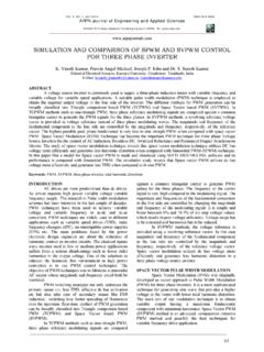
1 1LT34913491fa Cellular Phones PDAs, Handheld Computers Digital Cameras MP3 Players GPS ReceiversLi-Ion Driver for Four White LEDsWhite LED Driver withIntegrated Schottky in SC70and 2mm 2mm DFN Drives Up to Six White LEDs from a 3V Supply High Side Sense Allows One Wire Current Source Internal Schottky Diode One Pin Dimming and Shutdown 27V Open LED Protection Switching Frequency 5% Reference Accuracy VIN Range: to 12V Requires Only 1 F Output Capacitor Wide 300:1 True Color PWMTM Dimming Range 8-Lead SC70 Package Low Profile 6-Lead DFN Package(2mm 2mm )EfficiencyFEATURESDESCRIPTIOUAPPLICATIO SUTYPICAL APPLICATIOUCTRLVINL110 HVIN3V TO 5 VRSENSE10 3491 TA01aLT3491 SHUTDOWN ANDDIMMING CONTROLSWCAPLEDGNDC21 FC11 FC1: TAIYO YUDEN LMK212BJ105 MDC2: TAIYO YUDEN GMK316BJ105 MLL1: MURATA LQH32CN100 The LT 3491 is a fixed frequency step-up DC/DC converterspecifically designed to drive up to six white LEDs in seriesfrom a Li-Ion cell. Series connection of the LEDs providesidentical LED currents resulting in uniform brightness andeliminating the need for ballast resistors.
2 The devicefeatures a unique high side LED current sense that enablesthe part to function as a one wire current source; oneside of the LED string can be returned to ground anywhere,allowing a simpler one wire LED connection. TraditionalLED drivers use a grounded resistor to sense LED current,requiring a 2-wire connection to the LED switching frequency allows the use of tinyinductors and capacitors. A single pin performs bothshutdown and accurate LED dimming control. Few exter-nal components are needed: open-LED protection and theSchottky diode are all contained inside the tiny SC70 and2mm 2mm DFN packages. With such a high level ofintegration, the LT3491 provides a high efficiency LEDdriver solution in the smallest of CURRENT (mA)0 EFFICIENCY (%)5060203491 TA01b4051015807055654575 VIN = LEDs, LTC, LT and LTM are registered trademarks of Linear Technology Corporation. All other trademarks are the property of their respective voltage (VIN).
3 12 VSW voltage .. 32 VCAP voltage .. 32 VCTRL voltage .. 12 VConsult LTC Marketing for parts specified with wider operating temperature AXI U RATI GSWWWUPACKAGE/ORDER I FOR ATIOUUW(Note 1)LT3491 ESC8 LBXQTJMAX = 125 C, JA = 270 C/ WPARAMETERCONDITIONSMINTYPMAXUNITSM inimum Operating Current Sense voltage (VCAP VLED)VCAP = 30V 190200210mVCAP, LED Pin Bias CurrentVCAP = 16V, VLED = 16V2040 AVCAP, VLED Common Mode Minimum CurrentVCAP = 16V, VLED = 15V, CTRL = = 0V810 ASwitching Duty Cycle 8892%Switch Current Limit 260350mASwitch VCESATISW = 200mA200mVSwitch Leakage CurrentVSW = AVCTRL for Full LED CurrentVCAP = 30V to Shut Down IC50mVVCTRL to Turn On IC 100mVCTRL Pin Bias Current100nACAP Pin Overvoltage Protection 262728 VSchottky Forward DropISCHOTTKY = Leakage CurrentVR = 20V4 AThe denotes specifications which apply over the full operating temperature range, otherwise specifications are TA = 25 = 3V, VCTRL = 3V, unless otherwise CHARACTERISTICSSW 1 GND 2 GND 3 GND 48 CAP7 LED6 CTRL5 VINTOP VIEWSC8 PACKAGE8-LEAD PLASTIC SC70 LED voltage .
4 32 VOperating Temperature Range (Note 2) .. 40 C to 85 CMaximum Junction Temperature .. 125 CStorage Temperature Range .. 65 C to 150 CLead Temperature (Soldering, 10sec, SC-70).. 300 CTOP VIEWCTRLLEDCAPVINGNDSWDC PACKAGE6-LEAD (2mm 2mm) PLASTIC DFN4576321 TJMAX = 125 C, JA = 102 C/W, JC = 20 C/ WEXPOSED PAD (PIN 7) SHOULD BE CONNECTED TO PCB GROUNDO rder Options Tape and Reel: Add #TRLead Free: Add #PBF Lead Free Tape and Reel: Add #TRPBFLead Free Part Marking: PART NUMBERDC PART MARKINGLT3491 EDCLCHJORDER PART NUMBERDC PART MARKING3LT34913491faTYPICAL PERFOR A CE CHARACTERISTICS UWSwitch Saturation voltage (VCESAT)Schottky Forward voltage DropShutdown Current (VCTRL = 0V)Sense voltage (VCAP VLED)vs VCTRLOpen-Circuit Output ClampVoltageInput Current in Output OpenCircuitSwitching WaveformTransient Response(TA = 25 C unless otherwise specified)SWITCH CURRENT (mA)03503002502001501005001503003491 G0150100200400250350 SWITCH SATURATION voltage (mV)SCHOTTKY FORWARD DROP (mV)0 SCHOTTKY FORWARD CURRET (mA)15020025060010003491 G021005002004008003003504001200 VIN (V)0 SHUTDOWN CURRENT ( A)91215123491 G03630369 VCTRL (mV)0 SENSE voltage (mV)8012020003491 G0440050010001500240200160 VIN (V)0 OUTPUT CLAMP voltage (V)2728123491 G0526253693029 VIN (V)00 INPUT CURRENT (mA)
5 12345636 9123491 G06 VSW10V/DIVVCAP50mV/DIVIL100mA/DIVVIN = PAGE APPLICATION CIRCUIT200ns/DIV3491 G07 VCTRL5V/DIVVCAP5V/DIVIL200mA/DIVVIN = PAGE APPLICATION CIRCUIT1ms/DIV3491 G08 Note 1: Stresses beyond those listed under Absolute Maximum Ratingsmay cause permanent damage to the device. Exposure to any AbsoluteMaximum Rating condition for extended periods may affect devicereliability and 2: The LT3491E is guaranteed to meet performance specificationsfrom 0 C to 85 C. Specifications over the 40 C to 85 C operatingtemperature range are assured by design, characterization and correlationwith statistical process CHARACTERISTICS4LT34913491faQuiescent Current (VCTRL = 3V)Switching Current Limtvs Duty CycleSchottky Leakage Currentvs TemperatureOpen-Circuit Output Clamp Voltagevs TemperatureInput Current in Output Open Circuitvs TemperatureSwitching Frequencyvs TemperatureTYPICAL PERFOR A CE CHARACTERISTICS UW(TA = 25 C unless otherwise specified)Sense voltage (VCAP VLED)vs VCTRLS ense voltage (VCAP VLED)vs VCAPS ense voltage (VCAP VLED)vs TemperatureVIN (V)00 QUIESCENT CURRENT (mA) 9123491 G09 DUTY CYCLE (%)300 CURRENT LIMIT (mA)50150200250704503491 G10100504080609030035040025 CTEMPERATURE ( C) 500 SCHOTTKY LEAKAGE CURRENT ( A)3691215 25025503491 G1175100VR = 10 VVR = 16 VVR = 20 VTEMPERATURE ( C) 50 2525 OUTPUT CLAMP voltage (V)2730050753491 G1226292825100125 TEMPERATURE ( C) 50 INPUT CURRENT (mA)
6 45625753491 G1332 2505010012510 VIN = 3 VTEMPERATURE ( C) 50 FREQUENCY (MHz) (mV)00 SENSE voltage (mV)40801201602002405001000150020003491 G15 50 C25 C85 CVCAP (V)5 SENSE voltage (mV)200204253491 G16196192101520212208 TEMPERATURE ( C) 50 25192 SENSE voltage (mV)200212050753491 G17196208204251001255LT34913491fa1 + +RSW5 VINCAPQSDRIVER ++8 LED3491 F01 CTRLGNDPINS 2, 3, 476 +A = NUMBERS CORRESPOND TO THE 8-PIN SC70 PACKAGEUUUPI FU CTIO SSW (Pin 1/Pin 3): Switch Pin. Minimize trace area at thispin to minimize EMI. Connect the inductor at this (Pins 2, 3, 4/Pin 2): Ground Pins. All three pinsshould be tied directly to local ground (Pin 5/Pin 1): Input Supply Pin. Must be (Pin 6/Pin 6): Dimming and Shutdown Pin. Connectthis pin below 50mV to disable the driver. As the pinvoltage is ramped from 0V to , the LED current rampsfrom 0 to ILED ( = 200mV/RSENSE). The CTRL pin must notbe left (Pin 7/Pin 5): Connection Point for the Anode of theFirst LED and the Sense Resistor.
7 The LED current can beprogrammed by :ImVRLEDSENSE=200 CAP (Pin 8/Pin 4): Output of the Driver. This pin isconnected to the cathode of internal Schottky. Connect theoutput capacitor to this pin and the sense resistor fromthis pin to the LED PAD (NA/Pin 7): The Exposed Pad should besoldered to the PCB ground to achieve the rated DIAGRA WFigure 1. Block Diagram(SC70/DFN)6LT34913491faOPERATIOUT he LT3491 uses a constant frequency, current modecontrol scheme to provide excellent line and load regula-tion. Operation can be best understood by referring to theBlock Diagram in Figure power up, the capacitor at the CAP pin is charged up toVIN (input supply voltage ) through the inductor and theinternal Schottky diode. If CTRL is pulled higher than100mV, the bandgap reference, the start-up bias and theoscillator are turned on. At the start of each oscillatorcycle, the power switch Q1 is turned on. A voltage propor-tional to the switch current is added to a stabilizing rampand the resulting sum is fed into the positive terminal of thePWM comparator, A2.
8 When this voltage exceeds the levelat the negative input of A2, the PWM logic turns off thepower switch. The level at the negative input of A2 is set bythe error amplifier A1, and is simply an amplified versionof the difference between the VCAP and VLED voltage andthe bandgap reference. In this manner the error amplifier,A1, sets the correct peak current level in inductor L1 tokeep the output in regulation. The CTRL pin is used toadjust the LED current. The LT3491 enters into shutdownwhen CTRL is pulled lower than Output CurrentThe LT3491 can drive a 3-LED string at 2mA LED currentwithout pulse skipping using the same external compo-nents shown in the application circuit on the front page ofthis data sheet. As current is further reduced, the devicewill begin skipping pulses. This will result in some lowfrequency ripple, although the average LED current re-mains regulated down to zero. The photo in Figure 2details circuit operation driving three white LEDs at 2mAload.
9 Peak inductor current is less than 60mA and theregulator operates in discontinuous mode, meaning theinductor current reaches zero during the discharge the inductor current reaches zero, the SW pinexhibits ringing due to the LC tank circuit formed by theinductor in combination with the switch and the diodecapacitance. This ringing is not harmful; far less spectralenergy is contained in the ringing than in the 2. Switching WaveformsVSW10V/DIVIL50mA/DIVVIN = = 2mA3 LEDs200ns/DIV3491 F027LT34913491faAPPLICATIO S I FOR ATIOWUUUINDUCTOR SELECTIONA 10 H inductor is recommended for most LT3491 appli-cations. Although small size and high efficiency are majorconcerns, the inductor should have low core losses and low DCR (copper wire resistance). Somesmall inductors in this category are listed in Table 1. Theefficiency comparison of different inductors is shown inFigure 1. Recommended InductorsCURRENTLDCRRATINGPART( H)( )(mA) (TYPE D312C) 2 shows a list of several ceramic capacitor manufac-turers.
10 Consult the manufacturers for detailed informationon their entire selection of ceramic 2. Recommended Ceramic Capacitor ManufacturersTaiyo Yuden(800) (803) (714) PROTECTIONThe LT3491 has an internal open-circuit protection the cases of output open circuit, when the LEDs aredisconnected from the circuit or the LEDs fail open circuit,VCAP is clamped at 27V (typ). The LT3491 will then switchat a very low frequency to minimize input current. The VCAPand input current during output open circuit are shown inthe Typical Performance Characteristics. Figure 4 showsthe transient response when the LEDs are 3. Efficiency Comparison of Different InductorsCAPACITOR SELECTIONThe small size of ceramic capacitors make them ideal forLT3491 applications. Use only X5R and X7R types be-cause they retain their capacitance over wider temperatureranges than other types such as Y5V or Z5U. A 1 F inputcapacitor and a 1 F output capacitor are sufficient formost CURRENTThe LT3491 has a built-in Schottky diode.